This thread has been locked.

If you have a related question, please click the "Ask a related question" button in the top right corner. The newly created question will be automatically linked to this question.

TPS54561-Q1: Thermal Performance of the Application design in -20C to 80C

Part Number: TPS54561-Q1
Other Parts Discussed in Thread: TPS54561, TPS54561EVM-555

Hi,

We are planning to use the TPS54561-Q1 for our application to derive 5V from 8V to 13V input.
The output current requirement is 4A & we are planning to re-use the application design provided in the datasheet.
Our design must operate in condition with ambient temperature of -20C to 80C.

1. We had gone through the datasheet & we noted the following was mentioned in "Safe Operating Area" Section.
"Figure 47, through Figure 50 doesn't consider the impact from the catch diode thermal performance"

Was TPS54561 EVM kit with a different diode part (as opposed to PDS760-13 part in application design) used to plot the Safe operating curves?

2. We calculated the diode loss (for PDS760-13 which is used in the application design) with the help of equation 40 in the datasheet for 13V input , 5V 4A output which turns out to be 1.38719W.
With this value, we calculated the max ambient temperature for operation for this diode which came out to be 87.57C (only when considering Rth as 45, refer https://www.diodes.com/assets/Datasheets/PDS760Q.pdf).

Having said, If we closely follow the layout as in the EVM layout design, Will the design work in -20C to 80C ambient range without any issues? 

FYI, Our board is going to be mutli-layered board and we expect at least 2 GND planes in our design

Kindly let us know ASAP

Thanks,

Balaji

  • Hi,

    1. According to the datasheet, the test board of derating limits is similar to the TPS54561EVM-555 evaluation module, so you can refer to the board but it's hard to guarantee a same result.

    2. The theoretical values may have some variations on actual board, so you can have several actual tests on the evaluation module which you can apply it from ti.com before your design. If you have similar results, it will be more convincing.

  • Dear Iven,

    Thanks for your reply!
    Please find my inline replies.

    1. According to the datasheet, the test board of derating limits is similar to the TPS54561EVM-555 evaluation module,
    so you can refer to the board but it's hard to guarantee a same result.
    [Balaji] : I saw the following in the datasheet.
    "Derating limits apply to devices soldered directly to a double-sided PCB with 2 oz. copper, similar to the board on TPS54561EVM-555 evaluation module"

    - Is the double sided PCB the "test board" that you have mentioned?
    - Was the same design as in EVM(including diode) was soldered to double-sided PCB? If there is any difference, Can you please let us know on the same?
    - As the EVM is a four-layer board, Can I expected that the thermal performance of the EVM to be superior to that of the test board?
    - Will it be possible to share any design reference for the "test board" if you think it can help us.

    2. The theoretical values may have some variations on actual board, so you can have several actual tests on the evaluation module which you can apply it from ti.com before your design.
    If you have similar results, it will be more convincing.
    [Balaji] : We do not have this EVM at our end. Are there any details/results for temperature tests ran with TPS54561 EVM available for reference?

    Thanks,

  • Dear Iven,

    Can you please update?

    Thanks

  • Hi,

    1. As the EVM is a four-layer board I agree that it's very possible the thermal performance is better than the "test board", you can perform only one or two tests then you can verify it. And now we only have the EVM reference for this device.


    2. You can just apply an EVM from ti.com, it's the fastest way to verify it because it looks there is no such test data from our side. Thanks for you consideration.

  • Dear Iven,

    Thanks for your reply!

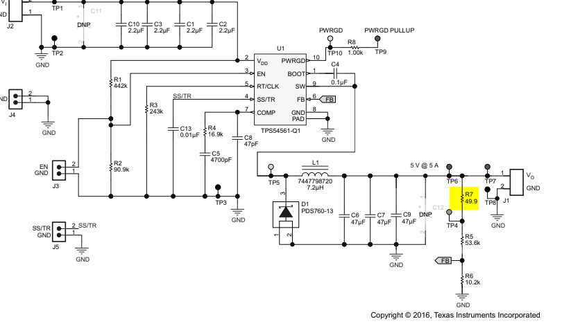
    We see that there is 49.9 Ohms resistor (R7) is present in the feedback divider of the EVM circuit(image attached). We hope this was added to measure the small-signal response and is not required to be used. 

    Please confirm on the same.

    Thanks,

    N.Balaji

  • Yes, that is there to connect the bode plotter transformer for measuring loop response.