Hi TI-team
My customer want to know the following about thermal information.
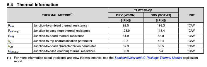
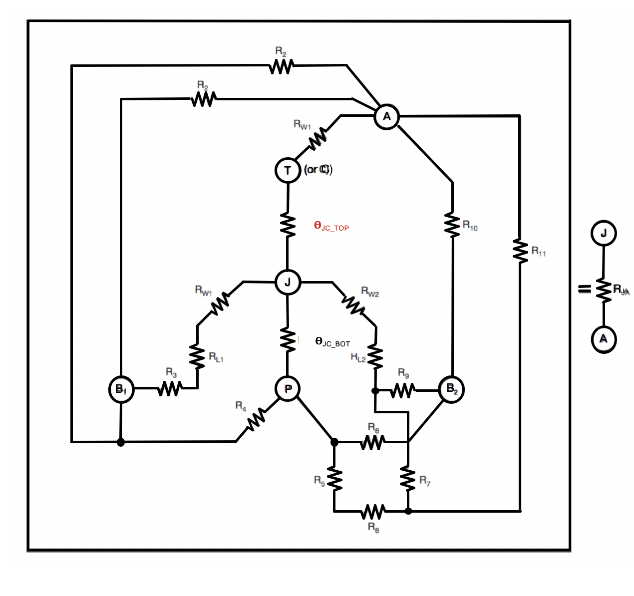
1.Do you have the items in this table [RθJA, RθJC(top), RθJB, ψJT, ψJB, RθJC(bot)] shown in the image diagram ?
2.What is the difference between RθJB and RθJC (bot) ?
3.The ΨJT of DRV is considerably smaller than the ΨJT of DBV.
Is there no problem ? Why small ?
Best Regards,
Koji Hayashi