This thread has been locked.

If you have a related question, please click the "Ask a related question" button in the top right corner. The newly created question will be automatically linked to this question.

TPS63030: Elevated VIN on TPS63030

Part Number: TPS63030

Hello,

We are using a TPS63030 adjustable regulator with feedback resistors for a VOUT of 3.3V

We have 3 x AA (1.5V) cells connected to VIN through a diode.
We also have VBUS (from a USB connector) connected to VIN through another diode.

With the USB cable removed then VBATT is in play.
With the USB cable connected then VBATT is over-ridden by VBUS (5V).

Thus the TPS63030 is powered from 4.5V of the batteries or 5V of USB (less the voltage drop of the associated diode).

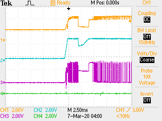
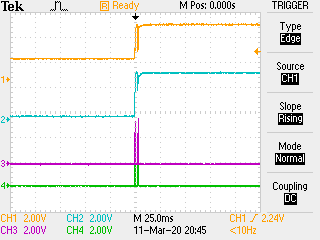
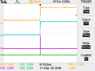
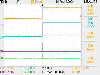
Under either condition (batteries only or batteries and USB) the voltage at the VIN pin is around 10V?

Is this normal?
If so why?

Thanks,
Mike

  • Hi Mike,

    This could happen if you have some kind of voltage source on the output side that is higher than the set output voltage, and the device is set to forced-PWM mode (PS/SYNC connected to GND). In that case the device will operate in reverse, and since you have blocking diodes on the input side, the input voltage will rise.

    Could you please post your schematic? What is the load in your circuit? Is there any voltage source on the output? 

    Could you also try running the converter with one source without the blocking diode, and see if the output voltage is correct?

    Best regards,
    Milos

  • Hello,

    The TPS63030 is the only power source.  This is what we have


    3xAA (4.5V) battery ---|>---------------[VIN TPS63030 VOUT]-------> (Vout=3.3V)
                                |     |                           |
    USB (5V) --------------|>----   [10uf]                      [10uf]
                                      |                           |
                                     GND                         GND


    -|>- are diodes.  When USB is connected it over-rides the battery.

    PS is tied low through a 1M resistor

    Mike

  • Hi Mike,

    Can you please show how the other pins are connected?

    Could you also try running the converter with only one source directly connected, without the blocking diode, and see if the output voltage is correct? Please test it without and with the load. 

    Best regards,
    Milos

  • Hello,

    Is there a way for me to upload images?

    Mike

  • Hello,

    With the battery connected directly to VIN (pin 5) we have VIN = 4.35V and VOUT=3.45V.  Under this condition VIN is not elevated.

    When VIN is connected to the battery through a diode then VIN is around 10V.  This is how it is connected in that instance

    • Between L1 (pin 4) and L2 (pin 2) is a 3.3uH inductor.
    • VIN (pin 5) and EN (pin 6) are tied together and are powered from the battery through a diode.
    • VINA (pin 8) has a 0.1uF capacitor connected between it and GND.
    • PS/SYNC is connected to GND through a 1 Meg resistor.
    • GND (pin 9), PAD (pin 11) and PGND (pin 3) are connected to GND.
    • Between VOUT (pin 1) and FB (pin 10) is a 1.1 Meg resistor.
    • Between FB (pin 10) and GND is a 198k resistor.
    • Between VOUT (pin 1) and GND are two 10uF capacitors in parallel.

    When VIN is less than 3.3V the TPS63030 operates in a step up mode and VOUT is 3.3V.

    When VIN is greater than 3.7V the TPS63030 operates in a step down mode and VOUT is 3.45V.

    When operating in a step down mode VIN of the TSP63030 is around 10V when VBATT goes through a diode to VIN.

    Is that normal?

    Mike

  • Hi Mike,

    You can upload images by clicking the "Insert/Edit Media" button when replying. 


    This behavior is not normal. Two possible causes are:

    1. Non-optimal PCB layout. Could you please post the PCB layout? Just a snippet of the area around the device, showing all layers, is enough.
    2. Failed part. Could you please replace the device and test the circuit again?

    In the meantime, I will test the TPS63030 on its EVM under the same conditions, with an input diode.

    Best regards,
    Milos

  • Hello,

    Here is the schematic

    Here is the PCB section

    Thanks,

    Mike

  • Hello,

    When the battery voltage (VBAT) is low enough such that the TPS63030 is operating in a step up mode VOUT/VDD is at 3.3V (as expected) and VIN is not elevated.

    When the battery voltage (VBAT) is high enough such that the TPS63030 is operating in a step down mode VOUT/VDD and VIN are elevated.  With VBAT at 4.5V, VIN is around 10V and VOUT/VDD is at 3.6V.

    Mike

  • Hi Mike,

    I tried to reproduce the issue on the bench, but as I expected, everything worked normal, regardless of which mode the device operates in.

    Your layout looks fine. Normally, we recommend VINA to be decoupled to GND via 100 nF, as it is done on the EVM:

    http://www.ti.com/lit/ug/slvu275/slvu275.pdf

    Did you try to replace the device and see if the issue still exists?

    If it is still there, could you please take scope plots during startup, to show the Vin rise, showing signals on VIN, VOUT, PS/SYNC and L1 pins.

    Best regards,
    Milos

  • Hello,

    We have two boards that behave the same.

    On one of the boards we disconnected VINA from VIN and added a 0.1uF capacitor between VINA and GND.  Same results.

    Did you place a diode between your power source and VIN on the board?

    If so what diode did you use?

    I will capture scope images and post them.

    Mike

  • Hello,

    The images below are the requested captures at three levels of VBAT (which connects to VIN via a diode).

    CH1 = VIN
    CH2 = VOUT
    CH3 = L1
    CH4 = PS/SYNC

    VBAT at 4.5V.

    VBAT at 4.0V.

    VBAT at 3.5V

    Should we have activity on L1 when in the step down mode?

    Thanks,
    Mike

  • Hi Mike, 

    I configured the device the same way you did (VINA to VIN, PS to GND via R/C, EN to VBAT), except for the inductor (1.5 uH, but that shouldn't affect the behavior). I am using a 20V/1A schottky diode (B120/B-13). I did not see any problems, regardless of the power mode (PS pin state), input/output voltages or output current.

    There is always activity on both L1 and L2 pins in power-save mode. In power-save mode, the device operates in bursts. During the bursts one pin goes high and the other actively switches, or both actively switch, depending on input/output voltages. 

    If VIN goes to 10 V, the device should fail, or stop when there is a voltage breakdown. In any case, if VIN goes to 10 V, that means that both input diodes should be off since Vbat and Vusb are <10 V. In that case the power can only come from somewhere else.

    1. Can you please show a scope plot for VIN, VOUT, L1 and L2 over a longer time, from startup until VIN reaches 10 V?
    2. Do you have any load on the output? From the scope plots I see that initially the output voltage rises to the nominal value, but after that there is a dip, as if something is turned on on the output?
    3. Do you have a board without this issue? If so, can you try A-B-A swap.

    Best regards,
    Milos

  • Hello,

    For some reason (I do not know why) we are not seeing 10V on VIN now.  However the output does not regulate when VIN is at 4.5V.  Here are some scope captures at difference durations.

    CH1 = VIN
    CH2 = VOUT
    CH3 = L1
    CH4 = L2

    We ordered the TPS63030 evaluation board, some new TPS63030 chips and some 1.5uH inductors.

    I will let you know if we get the same or better results.

    It looks like out TPS63030 might be damaged since there is no activity on either L1 or L2 when stepping down the voltage.

    Thanks,
    Mike

  • Hi Mike,

    Looking at the latest scope plots, I see two possibilities. Either the device is damaged and does not work for higher input voltages, or there is something on the output providing path to a voltage higher than 3.3 V. For example, if there is a pull-up path from VOUT to VBAT somewhere on the output/load, this would pull VOUT up and prevent the device from switching, so no activity on L1/L2. In power-save mode (PS pin connected to GND) this is expected behavior, and does not mean that the device is damaged.

    Double check with an evaluation module will help. In the meantime:

    1. In your previous tests (scope plots), do you have anything connected to the output of the converter?
    2. Can you check VOUT with PS/SYNC connected to VIN (therefore putting the device into forced-PWM mode) and apply 4.5 V to input?

    Best regards,
    Milos

  • Hello,

    1. The rest of our circuit is connected to the out put of the TPS63030.

    2. In the captures above PS/SYNC is connected to VIN before and after 4.5V is applied.

    I will test with VOUT not connected to the rest of the circuit and let you know what I find.

    Thanks,
    Mike

  • Hello,

    You were right, I was wrong. There was a diode in backwards that was feeding VBATT to VDD.

    We are all good now.

    Thank you for helping us through this.

    Mike

  • Hi Mike,

    Great. I will then close the thread, if you have more questions just post a reply below, or create a new thread if this one gets locked.

    Best regards,
    Milos