This thread has been locked.

If you have a related question, please click the "Ask a related question" button in the top right corner. The newly created question will be automatically linked to this question.

BQ24715: bq24715 schematic doubt

Part Number: BQ24715

Hi,

We are using bq24715 as a charger IC

While making the schematic for the same, I had a doubt regarding the ground connections.

From the application circuit in the datasheet, the ground is represented by 2 symbols

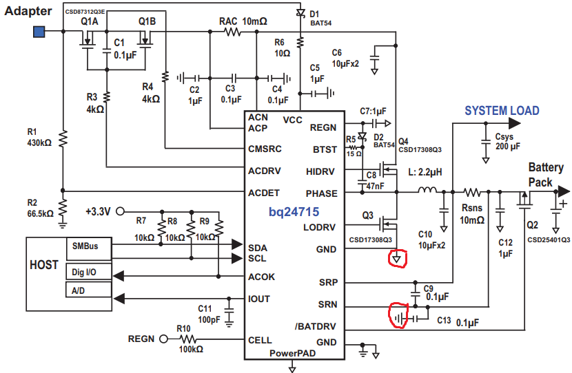
 is there any specific reason for having two different representations?

Can i connect common ground for all of them ( which has down arrow)?


Thank-you

Warm Regards

Harini Krishna

  • Hey Harini,

    The two connection symbols for GND represent a distinction between a power ground and a signal ground.

    Power ground is the solid triangle GND symbol and signal/reference ground is the dashed triangle GND symbol. 

    We recommend this to avoid the noisy power ground from influencing the critical signal pins and ground references. 

    Regards,

    Joel H

  • Hi Joel,

    Thank-you for the reply

    How do we separate the power ground and common ground on the PCB? Is it by having different netlables?

    It would be very helpful if  you provide a reference PCB layout?

    Thank-you

    Warm Regards

    Harini Krishna

  • Hey Harini,

    The best schematic reference we have is from the BQ24715EVM user's guide here: http://www.ti.com/lit/ug/sluua74/sluua74.pdf

    However, it is not a very good reference for your question above.

    Typically, yes you have two different net names, and you can have a pseudo-device (our Altium PCB/Schematic editor tool has a component called a "Net-Tie") which ties nets together. Some customers use a 0-Ohm resistor because the signal/analog ground should not process current, so there is no power dissipation concern.

    Regards,

    Joel H