Because of the Thanksgiving holiday in the U.S., TI E2E™ design support forum responses may be delayed from November 25 through December 2. Thank you for your patience.

This thread has been locked.

If you have a related question, please click the "Ask a related question" button in the top right corner. The newly created question will be automatically linked to this question.

UCC21530: Continuous Conduction mode

Part Number: UCC21530
Other Parts Discussed in Thread: SN6505B, UCC23513

Hi,

I need UCC21530 to switch 100V through a high side NMOS and low side NMOS to provide Ground as per the attached schematic. The high side NMOS is continuously ON continuously and OFF for a duration of 3ms when needed (actual circuit using a microprocessor based on a logic).

I tried to simulate but I get errors and the OUTA does not switch to OFF. Attached is the circuit. Can you tell me what I am doing wrong?

Thanks,

PKUCC21530_TRANS_Edit.TSC

  • Hi Pratap

    Thank you for your question. I work on the applications team in the high power drivers group.

    I think your primary challenge is coming from the slow switching frequency combined with the high-side bootstrap supply. At a circuit level, Bootstrap supplies need higher switching frequency in order to be constantly replenished, otherwise Cboot runs out of charge and the gate driver turns off. If you really need to switch at such low frequencies, I recommend using some kind of isolated supply, such as SN6505B to provide the high-side bias. For purposes of simulation, you can just place a floating supply from VDDA-VSSA.

    At a simulation level, this model needs the TR maximum time step in the Tools->Analysis Parameters menu to be much smaller. It’s kinda strange and I’m not exactly sure why, but at its default value of 10G, it allows the model to step through in ~300us increments which is why OUTA does not respond to the input immediately. Lowering the TR maximum time step to 50ns allowed the model to respond correctly and simulate the output. It runs much slower, though, since you’re still simulating 200ms - took about ~5 minutes on my laptop.

    If this answered your question, could you please press the green button? If not, feel free to ask more questions.

    Thanks and best regards,

    John

  • Hi,

    Thanks for the response. I was having the same doubt. Can I go with something like DCP0205 for the isolated power?

  • Hi Pratap,

    I'm honestly not too familiar with those devices. It looks like the DCP0205 is only designed for functional isolation and should not be used for reinforced isolation, like UCC21530. If you only need functional isolation (ie. just need a high-voltage half bridge driver), then it looks like the DCP0205 should be just fine, assuming it meets your power requirements.

    Thanks,

    John

  • Hi John,

    DCP0205 is for the supply that feeds the bootstrapped capacitor used in UCC21530. This isolated supply was suggested by you in the earlier reply since my switching frequency is low. Now with this, will this part suffice for my application?

    Thanks,

    Pratap

  • Hi Pratap,

    I mentioned the SN6505B because it is more configurable you can select the proper transformer for the gate drive bias that you want. You can see how this is implemented in this reference design:

    https://www.ti.com/tool/PMP21561

    I mainly hesitate to recommend the DCP0205 because it only lists signal isolation and ground bounce protection as its features, and does not list common-mode transient immunity. These fast switching, high voltage circuits need high CMTI in order to function properly. The SN6505B push-pull can handle that since the push-pull transformer has low CIO.

    Thanks,

    John

  • Hi John,

    Thank you.

    So if I use the SN6505B, then I will not need the bootstrap diode and capacitor. Am I correct?

    Thanks,

    Pratap

  • Pratap K said:

    So if I use the SN6505B, then I will not need the bootstrap diode and capacitor. Am I correct?

    Hi Pratap,

    You are correct.

    Best,
    Dimitr

  • Hi,

    Thank you for the support. I have made improvements and addition to my design thus far.

    We have a new requirement that the circuit must be able to tolerate reverse voltage application. 

    I have attached the latest circuit that I am working with. My plan is to use two N-FETs in back to back combination.

    1. Will UCC21530 withstand the reverse voltage? Max Reverse voltage of 70V applied between "Vout" and ground.

    2. Another option I see is to float the Bottom NFET (U3). U3 is intended to work as a pull down switch. Do you foresee any issue?

    Let me know if you have any other comment on the circuit. UCC21530_TRANS_Edit-0401.TSC

  • Hi Pratap,

    Can you help draw a schematic with the intended voltages applied?

    UCC21530 has a 30V absolute maximum between VDDA-VSSA and 30V absolute maximum between VDDB-VSSB. The voltage between VSSA and VSSB nodes can be much higher. It can also be positive or negative.

    If the bottom NFET is floating, how will it pull VOUT down to GND?

    Thanks,

    John

  • 3365.UCC21530_TRANS_Edit-0401.TSCHi John,

    I have attached two files: one is the simulation file and second is the word document showing application of the fault voltages (RED Arrow).

    The circuit has to be protected against these fault voltage applications.

    I am planning to go with back to back FETs to protect them. My concern is on the UCC21530.

    Also,

    1. Is there a way to simulate different grounds in TINA TI?

    2. I tried to simulate the following and the simulator threw an error: 

      2a. VSSB and bottom NFET isolated (floating)

      2b. VSSB isolated (floating) and bottom NFET grounded. 

    3. Will separating the grounds - logic input, VSSA and VSSB grounds help in the fault voltage scenario?

    Fault Voltages.docx

  • Hi Pratap,

    I have found that simulators do not do a great job of simulating with nodes in a 'floating' configuration. They generally need to start at some reference voltage in relation to one other. With that in mind, you can either add a voltage source from the input side GND to the output side GND to establish this reference. You could also just put a very small capacitor and set the starting voltage to 0 to establish a reference level.

    On the second question, it looks like the simulation is likely throwing an error because you are wiring V7, V8, and V9 in series with each other, creating a loop of voltage sources. These sources would try to push infinite current (70V+70V+70V = 210V) since 210V/0Ohms = Infinite current.

    I would recommend that you just try to turn your HV DC supply from +80V to -80V to test the reverse voltage handling capability.

    Based on my understanding, UCC21530 should be okay with this negative voltage handling, as long as the power supplies to the gate drivers are isolated and prevent VDDx-VSSx voltage from going beyond recommended maximum specifications.

    Thanks,

    John

  • Hi John,

    I am trying to safeguard the FET by back-to-back configuration. But it is not working. Do you have a reference circuit using UCC21530?

    Thanks,

    Pratap

  • Hi Pratap,

    Usually, reverse supply protection is put in between the DC bus supply, and the DC bus caps. This can either be a diode, or an active circuit which can detect reverse current and shut off the flow of current. Something like seen in this tech note.

    http://www.ti.com/lit/an/slva139/slva139.pdf

    Can you please give me more context as to what your circuit is doing? There are many ways to safe guard against reverse current protection, but it is usually always done before the power stage. I have never seen it done in the power stage, usually because it adds extra cost and extra loop inductance to your switch loop. If you can draw me a simple diagram of what type of system this circuit needs to interface with, I may be able to help further.

    Thanks,

    John

  • Hi John,

    Attached is the block of circuit that I am working with. I need to protect my circuit when IN and OUT are reversed. Diode in the path is ruled out due to high dissipation (50A). I tried simulating a circuit with back-to-back MOSFET with common source. I get convergence issue sometimes and it shows as the MOSFET turns ON. Can you suggest what I maybe doing incorrect?

    Is it possible to have back-to-back Mosfet in half bridge drive?

    Thanks,

    Pratap

    1030.Circuit.docx

  • Hi, Pratap,

    I work with John on our drivers team. Let me jump in here.

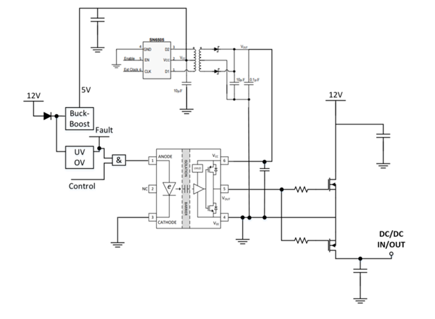
    This might be a simpler implementation for what you are trying to accomplish, if I understand correctly. The idea behind this circuit is the SN6505B drives a transformer to provide an isolated supply for the UCC23513. This allows the output to remain high indefinitely, since we aren't relying on a bootstrapping technique. Maybe this would work in your application as well?