This thread has been locked.

If you have a related question, please click the "Ask a related question" button in the top right corner. The newly created question will be automatically linked to this question.

TPS549B22: RSP/RSN Feedback & PGOOD

Part Number: TPS549B22
Other Parts Discussed in Thread: TPS549D22, TPS546D24A, TPS546A24A

I am using the TPS549B22 1.5-V to 18-V VIN, 4.5-V to 22-V VDD, 25-A SWIFT Synchronous Step-Down Converter With Full Differential Sense and PMBus. I was wondering if it is possible to change between output voltages with the PMBUS. I need a 1.25V output and a 3.3V output. Only one has to be on at a time. In addition, while reading the TPS549B22 datasheet, I was confused on the following sections:

7.5.2.1 RSP/RSN Remote Sensing Functionality (How do I select the correct feedback resistor values?)

7.5.2.2 Power Good (PGOOD Pin) Functionality (What is this pin used for? Is it a vital part of the design? This section does not make sense to me.)

I would really appreciate if someone could clear up these sections for me as well as let me know if the two output configuration is possible with this IC. Thanks!

  • Hi Andrei,

        Just a couple of questions for us to get clarity on your application.

    Do you mean that you will change Vout from 1.25V to 3.3V? What is the load that you are driving? What is the current drawn by the load?

    When you mean "only one has to be on at a time", were you looking to have power switches to turn on/off the voltages to the appropriate loads?

    Can you give us more insight into your application so that we can help answer your questions appropriately?

    Regards,

    Gerold

  • Hi Gerold,

    Background Information: 

    I am a senior at Arizona State University. I have partnered with Honeywell for my capstone project. They gave me a list of requirements and asked me to create a step-down power supply that uses the TPS549B22 IC. The power supply must be able to switch between Vout = 1.25V and Vout = 3.3V based on user input through the PMBUS. Only one of the outputs will be active at a time. For example, the user will use the 1.25V output to power a specific load. Then he will switch out the load and change the voltage to 3.3V using software commands. The max load current draw is 4A for the 1.25V output and 3A for the 3.3V output. Let me know if you want more information or have any questions. Thank you for your help/time. 

    Regards, 
    Andrei Marinescu
    The Luminosity Lab | Student Researcher 
    Ira A. Fulton Schools of Engineering | Arizona State University
  •  

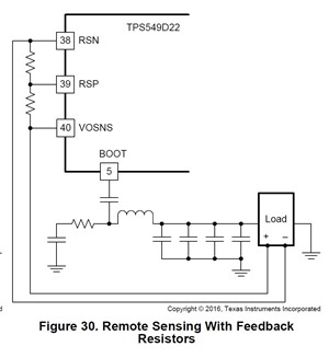
    The TPS549D22 power IC has some limitations to its internal reference voltage that make generating a 1.25V and 3.3V output from the same physical schematic without changing external components challenging.  The internal reference voltage is limited to 1.2V, and generating output voltages greater than 1.2V is accomplished by using an external resistor divider across the output voltage and sensing the differential voltage across the lower resistor if this divider.

    The TPS549D22 uses TI's D-CAP3 control mode, which is a variation of Constant On-Time (COT) control.  The TPS549D22 will adjust its operating frequency to attempt to regulate the voltage between Remote Sense Positive (RSP) and Remote Sense Negative (RSN) to be equal to the internal reference voltage.  With a maximum RSP to RSN voltage of 1.2V, you would need resistors with a ratio of (3.3 - 1.2) : 1.2 = 2.1 : 1.2 = 1.75 :1

    For example, if the resistor from RSP to RNS = 10k-Ohms, the resistor from VOSNS to RSP should be 17.5k-Ohms, that way when RSP - RSN = 1.2V, VOSNS - RSN will be 1.2V x (1 + 17.5k / 10k ) = 3.3V

    The problem here is getting VOUT down to 1.25V with this feedback divider, as that would require setting the reference voltage to 0.454V (1.25V / (1+17.5k / 10k) = 0.454V and the TPS549D22 does not allow the reference voltage to be set that low.  The programmable range of the reference voltage of the TPS549D22 is only 0.5996 V to 1.1992 V

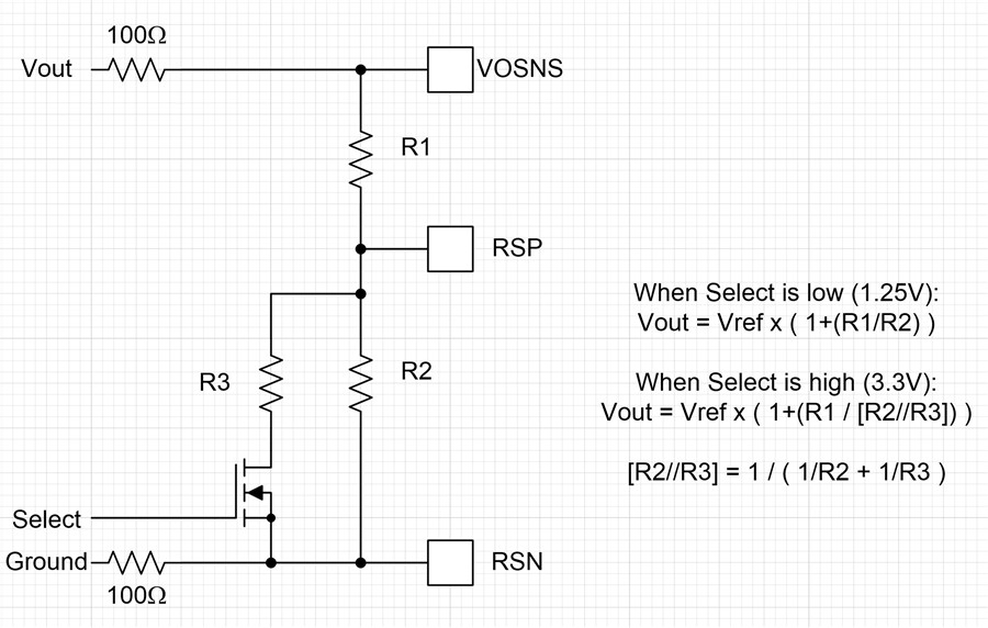
    To get this range of adjustment, you will need to change the resistors used to divide the output down to the reference voltage.  The typical way to do that would be to have a second resistor from RSP to RSN in series with an N-channel MOSEFT so that the two resistors work in parallel when the MOSFET is ON.  The MOSEFT is ON the parallel combination of the RSP to RSN resistors generate a divider that meets the ratio needed to generate 3.3V and when the MOSFET is off, the single resistor from RSN to RSP meets the ratio needed to generate 1.25V.

    If that works, I can help you select the correct resistors.

    Because the resistors needed to generate 1.25V from a 1.2V reference are very large and prone to leakage errors, I would recommend using a lower reference voltage to program the 1.25V and 3.3V values if you plan to use this approach.  The 0.8008 or 0.7500 V reference could be convient options.

    The resistor ratio is R1 / R2 = (Vout/Vref - 1) where R1 is the resistor from VOSNS to RSP and R2 is the resistor from RSP to RSN

    Since you want to have a common R1 you'll need 2 different R2 Values, the equation is R2 = R1 / (Vout-Vref - 1)

    For Vref = 1.1992  @ 1.25V R2 = 23.6x R1 and @ 3.3V R2 = 0.571x R1

    For Vref = 0.8008 @ 1.25V R2 = 1.783x R1 and @ 3.3V R2 = 0.320x R1

    For Vref = 0.7500 @ 1.25V R2 = 1.5x R1 and @ 3.3V R2 = 0.294x R1

    An alternate solution would be to select a different high-current integrated FET Synchronous BUCK converter that can support the adjustable range from 1.25V to 3.3V without changing external components, such as the TPS546D24A which uses an internal feedback divider so that the output voltage can be programmed from 0.25V to 6V.

    As for the Power Good Pin, this is a standard Power indicator signal.  It provides an open-drain drive signal that indicates when power is good, or bad.  When Power is "not good" the TPS549D22 turns on a low-resistance FET to pull the PGOOD pin low, and when Power is good - no faults detected, soft-start complete and the output voltage is within a specified range of the target regulation voltage, the device turns this pull-down FET off, releasing the PGOOD voltage to be pulled-up by an external resistor or pull-up current source.

    Power Good pins are commonly used for sequencing in multi-rail systems.  The Power Good of one device can be connected to the Enable of another device to ensure that they power-up in the correct sequence, and to ensure that the second power supply is disabled should the first power supply experience a fault condition.  If it is not needed for other system level requirements or sequencing, the PGOOD pin can be connected to the BP pin with a 10k - 100k resistance.  Some designers will add a red LED in series with a resistor so that the LED is illuminated when a fault occurs to assist with debug efforts.

  • Gerold,
    Thank you very much for the descriptive and helpful feedback!
    In regards to the N-channel MOSFET altering the voltage divider to meet both output voltages, how would this MOSFET be triggered? I understand the concept, but I am confused how this MOSFET will be triggered when 1.25V is needed as an output voltage. 
    In addition, how can I implement the red LED on the PGOOD pin? Do I disconnect the PGOOD pin from the BP pin and tie an LED (with a resistor) from PGOOD to GND?
    If you have spare time, I would appreciate it if you drew these two circuits because I am a little confused how to setup the MOSFET ( for RSP/RSN) and LED (for PGOOD). I appreciate your patience and expertise! 

    Regards, 
    Andrei Marinescu
    The Luminosity Lab | Student Researcher 
    Ira A. Fulton Schools of Engineering | Arizona State University
  •  

    It's Peter actually.

    Here is the circuit for controlling two discrete output voltages with an N-channel FET to switch between the two value.  The gate of the N-channel FET would need to come from somewhere else depending on what is selecting 1.25V or 3.3V.

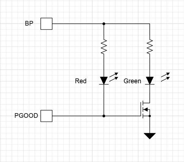
    For Power Good, here is a circuit that will turn on a red LED when Power is "bad" and a green LED when Power is Good.

    When power is "Bad" the PGOOD pin is pulled low by the open-drain pull-down, turning the MOSFET off and forcing current through the red LED.  When power is good, the PGOOD pull-down is turned off, the Red LED turns off and the gate of the MOSFET is pulled up, pulling current through the green LED and turning it ON.

  •  

    As I previously mentioned, the TPS549D22 will not adjust the output voltage from 1.25V to 3.3V purely through the PMBus interface, the reference voltage does not provide that much dynamic range.  You would need to have some additional control to drive the N-channel FET, most likely using whatever signal is being used to switch between the two "loads"

    If that is not possible, and you need to be able to switch between 1.25V and 3.3V purely through PMBus, I would suggest that the TPS546A24A would be a better choice.  It's internal divider and programmable reference would allow switching between 1.25V and 3.3V purely through the PMBus digital communication.