Other Parts Discussed in Thread: LM25118
We have always been very helpful.
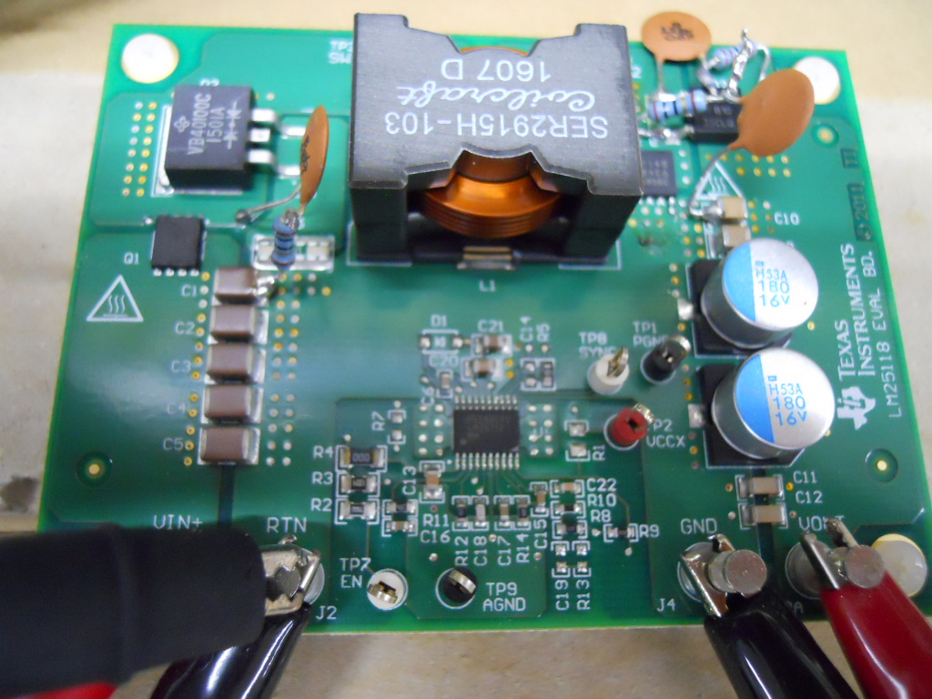
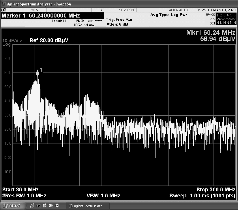
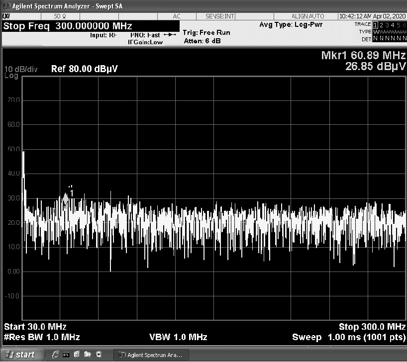
What are the recommended countermeasures for radiation noise during operation?
The oscillation frequency is 300kHz.
Take measures.
This thread has been locked.
If you have a related question, please click the "Ask a related question" button in the top right corner. The newly created question will be automatically linked to this question.
Hello user6144845
Thank you for using the LM25118 and reaching out with your questions.
In the frequency range of 30MHz to 1GHz the rising and falling of the switch node and any high frequency ringing can affect the measurements.
One suggestions is to slow down the switch node by adding an RC snubber to the switch node or adding gate resistance to the MOSFET to slow down the turn on time. A snubbber across the output diode can also help dampen any high frequency ringing.
Please let me know if you have any questions.
Thanks,
Garrett
Hello. Mr. Garrett
Thank you very much for the answer.
Ringing was observed when measuring the switching waveform (TP3) of the LM25118EVAL.
As an improvement method
Insert CR (5 to 10Ω + 1,000PF to 10,000PF) between the source and GND of FET Q1.
CR (5-10Ω + 1,000PF-10,000PF) was inserted between the drain and source of FET Q2.
The ringing waveform does not change much and appears as radiated noise.
Please let us know if you have any other suggestions for improvement.
Please show the schematic.
The ringing frequency is about 50MHz.
Thank you.
Hello. Mr. Garrett
Inserting a snubber between the drain and gate of the FET did not improve the ringing of the switching waveform.
When checking the waveforms of the HO and LO pins of the LM25118, there was ringing. When a snubber circuit was inserted between the gate of the FET and GND, the ringing almost disappeared, and the efficiency decreased by about 1 to 2%. Could be improved.
Please let us know if you have any comments.
Thank you very much.
Hello,
For noise that is occurring at in this frequency range layout is very important. The snubbers should be placed such that the parasitic inductance is minimized. Typically this is done with surface mount devices. These surface mount device should be place directly across the switching device. RC snubber should be place arcoss the drain to source of a MOSFET and the anode and cathode of a diode.
When the snubber is connected to the gated drive this is effectively adding some impedance slowing down the rise and fall time of the switch node reducing high frequency ringing. The same thing can be implemented with a simple gate resistor. Slowing down the rising and falling of the switch nodes will increase the switching losses, impacting efficiency. There is no way around this.
Please let me know if you have any questions.
Thanks,
Garrett