This thread has been locked.

If you have a related question, please click the "Ask a related question" button in the top right corner. The newly created question will be automatically linked to this question.

TPS53219A: Input inrush current estimation

Part Number: TPS53219A
Other Parts Discussed in Thread: TPS563219A

Hi Sir,

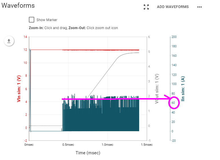
       Is it possible to estimate or calculate the input inrush current from the circuits of TPS53219A and output load?

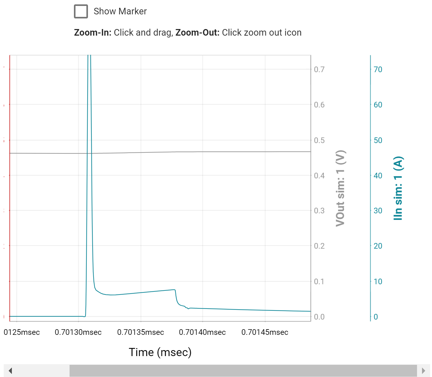
       After trying to simulate the startup on WEBENCH, just found the waveform of input inrush current is weird and up to 60~80A.

       Is this the same in practical application?


Thanks

Sincerely,

Edward


  • If you zoom into the Iin current,  you see the short duration spike of current.   The default on the source impedance is 1mOhm, you can increase the resistance to 10mOhm and minimize the spike.   

  • Hi David,

        Thanks for your feedback.

         I tried to increase the source impedance to 10mohm and the input inrush current decreases to around 12A.

         Just have two more questions.

          (1) Even with 10mohm, the input inrush current is still about 10~12A. Will this amplitude of inrush current affect the operation of TPS53219A?

          (2) There are many pulses of inrush current. Is the phenomena normal? 

               We just saw the same waveform from other E2E post.

    https://e2e.ti.com/support/archive/internal/int-non-isolated_dcdc/f/198/t/462157?tisearch=e2e-sitesearch&keymatch=tps53219%20inrush

    Thanks for your advice.

    Sincerely,

    Edward

  • Hi Edward,

    The inrush current in a real application is impacted by many factors like VIN/VOUT, L and Cout, loading condition, and impedance (like inductor DCR, high side Rdson, PCB board resistance) in the loop. You need consider those factors when you do some simulation. Typically we don't need to focus on the inrush current, the TPS563219A has a SS pin, which could adjust the soft start time to flatten the inrush current if need.

  • As Ryan is stating the simulations are idealized, minimum parasitic elements are used to speed up simulations.

    The source in the simulation is an ideal voltage with a series resistance.  On a pcb, the source

    will not be an ideal source with a resistor.   It will have resistance, inductance and a response time to transients.    The parasitic inductance will minimize the current spikes. 

    The TPS53219A is a switch mode power supply.  The high side mosfet turns on and

    passes current from the input to the output.  see figure 2 in http://www.ti.com/lit/an/slyt670/slyt670.pdf

    Simulations are useful, but sometime misled because of the simplifications to speed up the simulation.


  • Hi David and Ryan,

             Thanks for your detailed explanation. 

             I think if we implement delay start (pin EN) and soft-start (pin MODE), these will also help to reduce the magnitude of inrush current.

    Thanks

    Edward