This thread has been locked.

If you have a related question, please click the "Ask a related question" button in the top right corner. The newly created question will be automatically linked to this question.

WEBENCH® Tools/TPS53318: Device not switching

Part Number: TPS53318

Tool/software: WEBENCH® Design Tools

Hi,

I have used Webbench power designer to design a 5V regulator using the TPS53318 part. Schematic is attached.

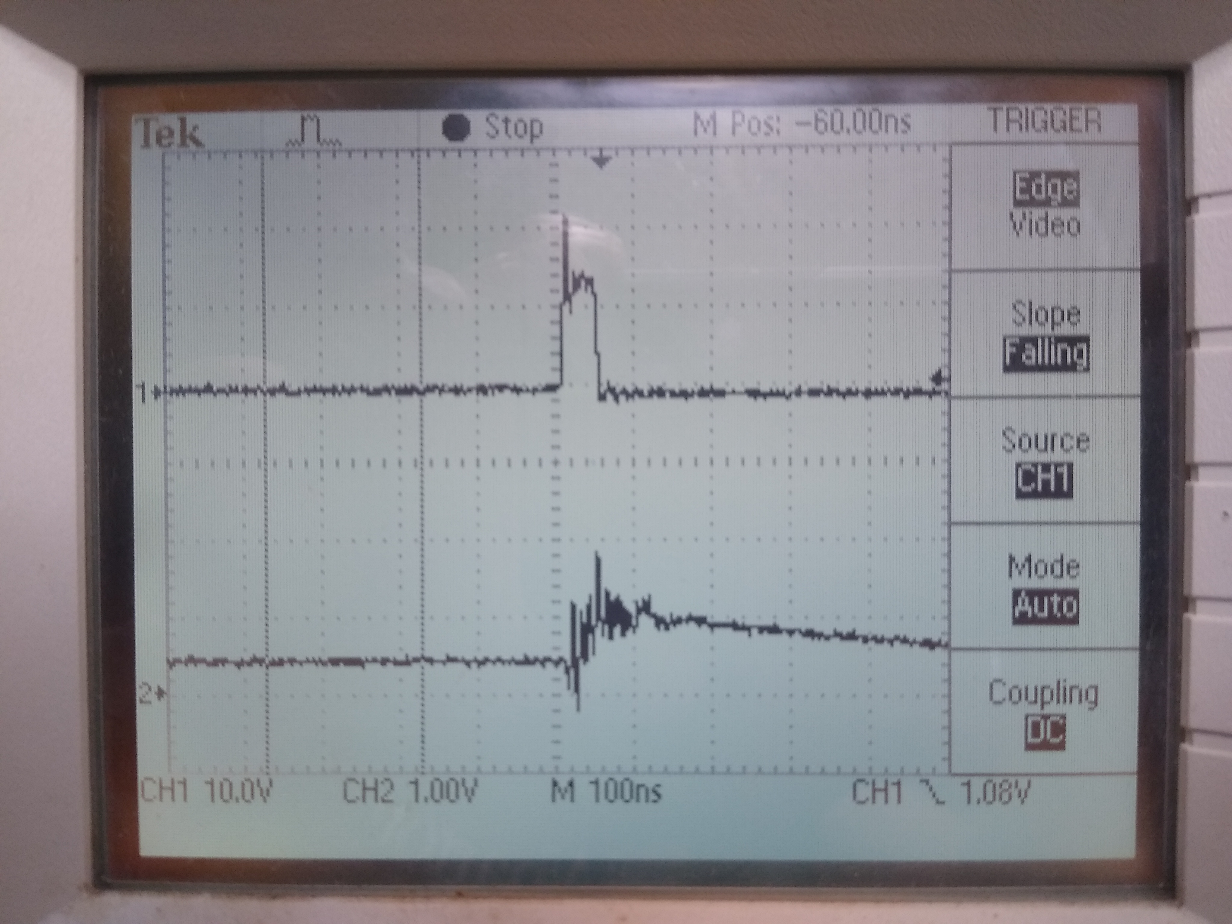
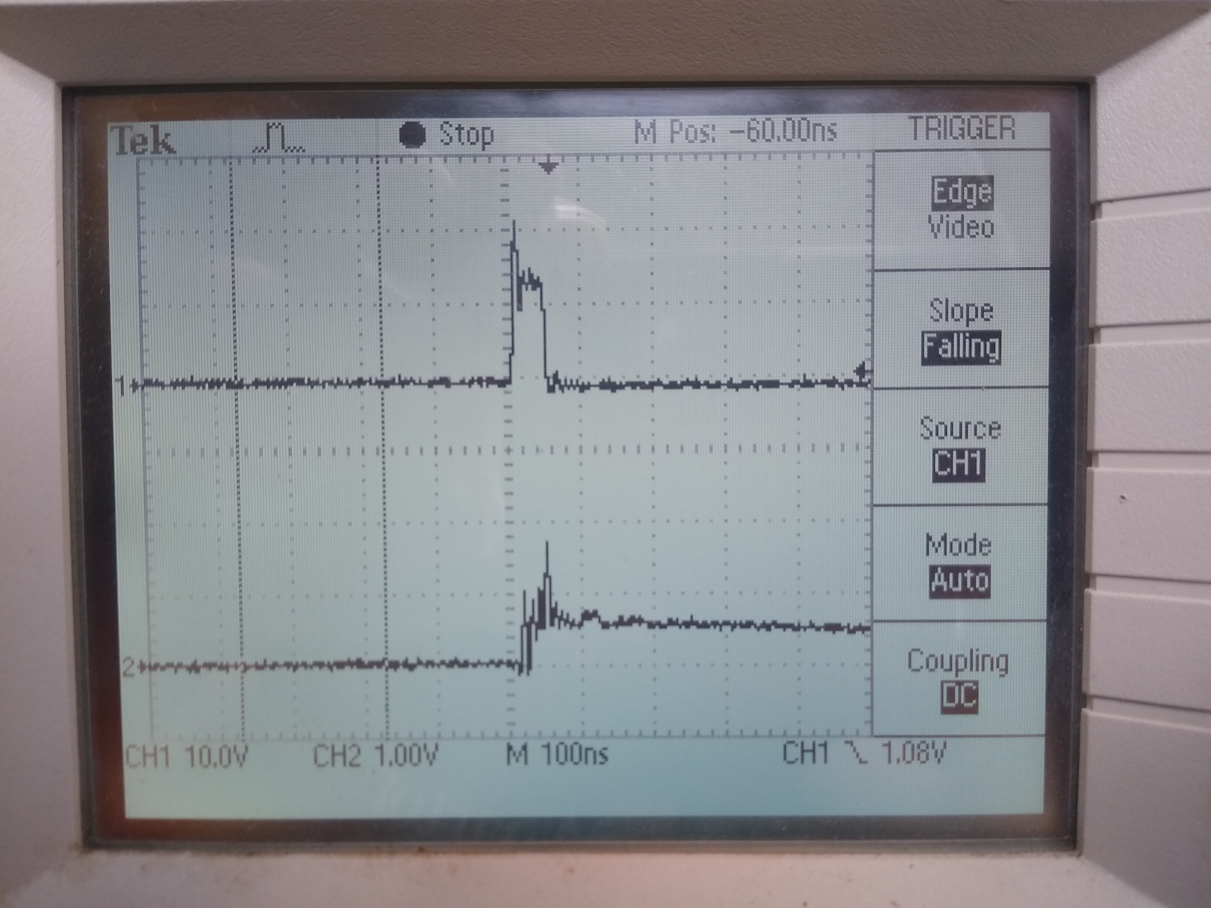
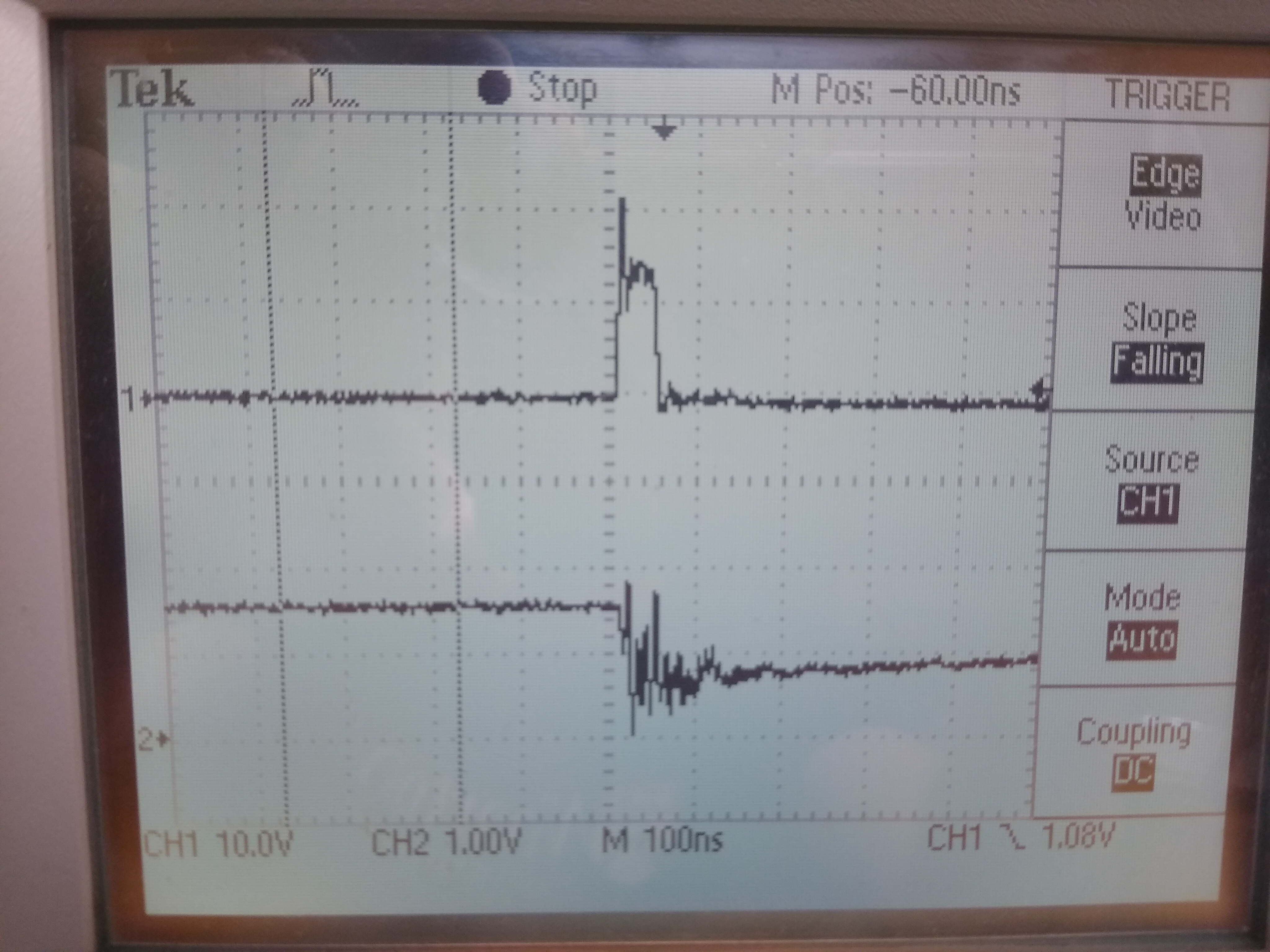
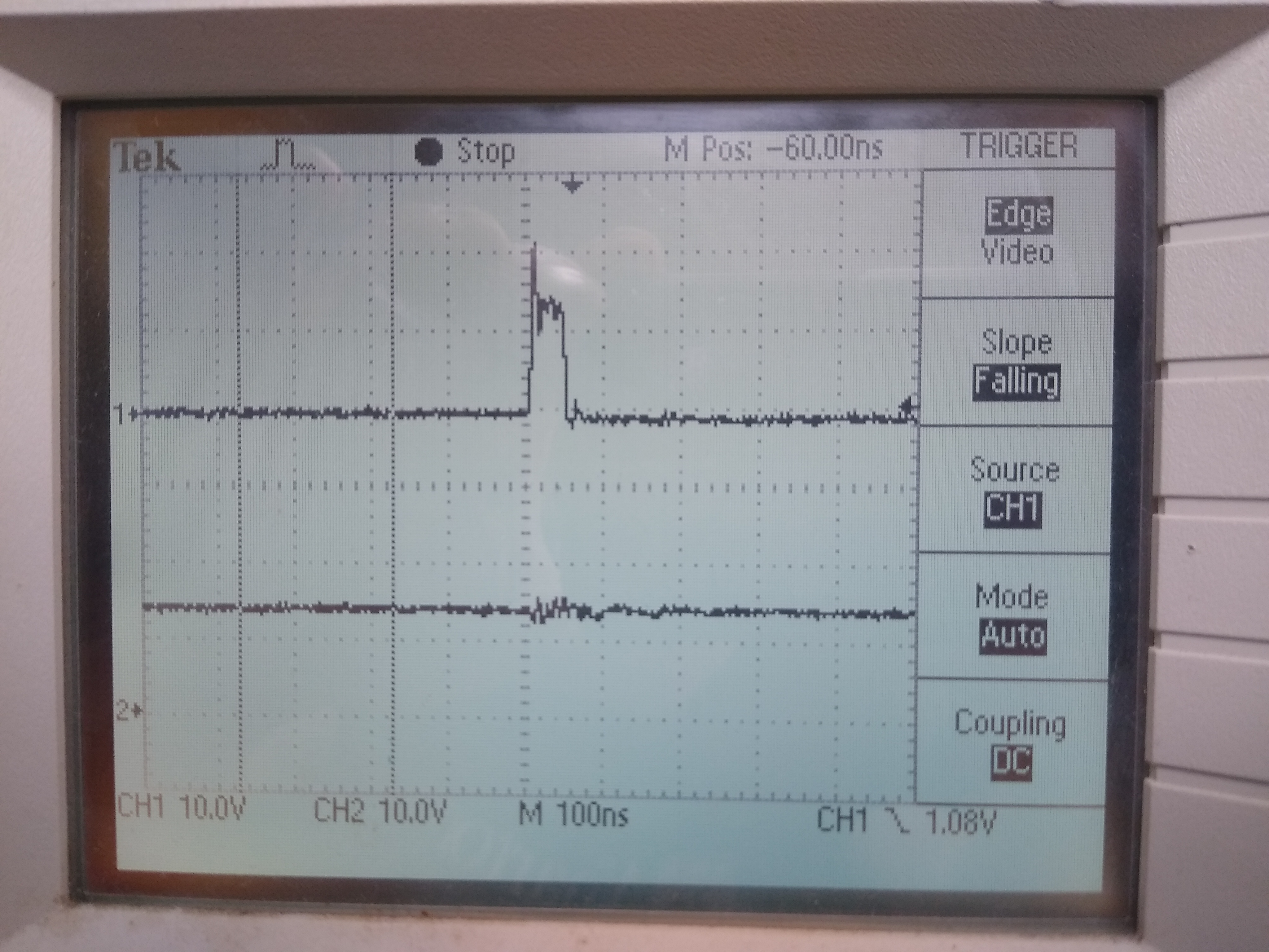
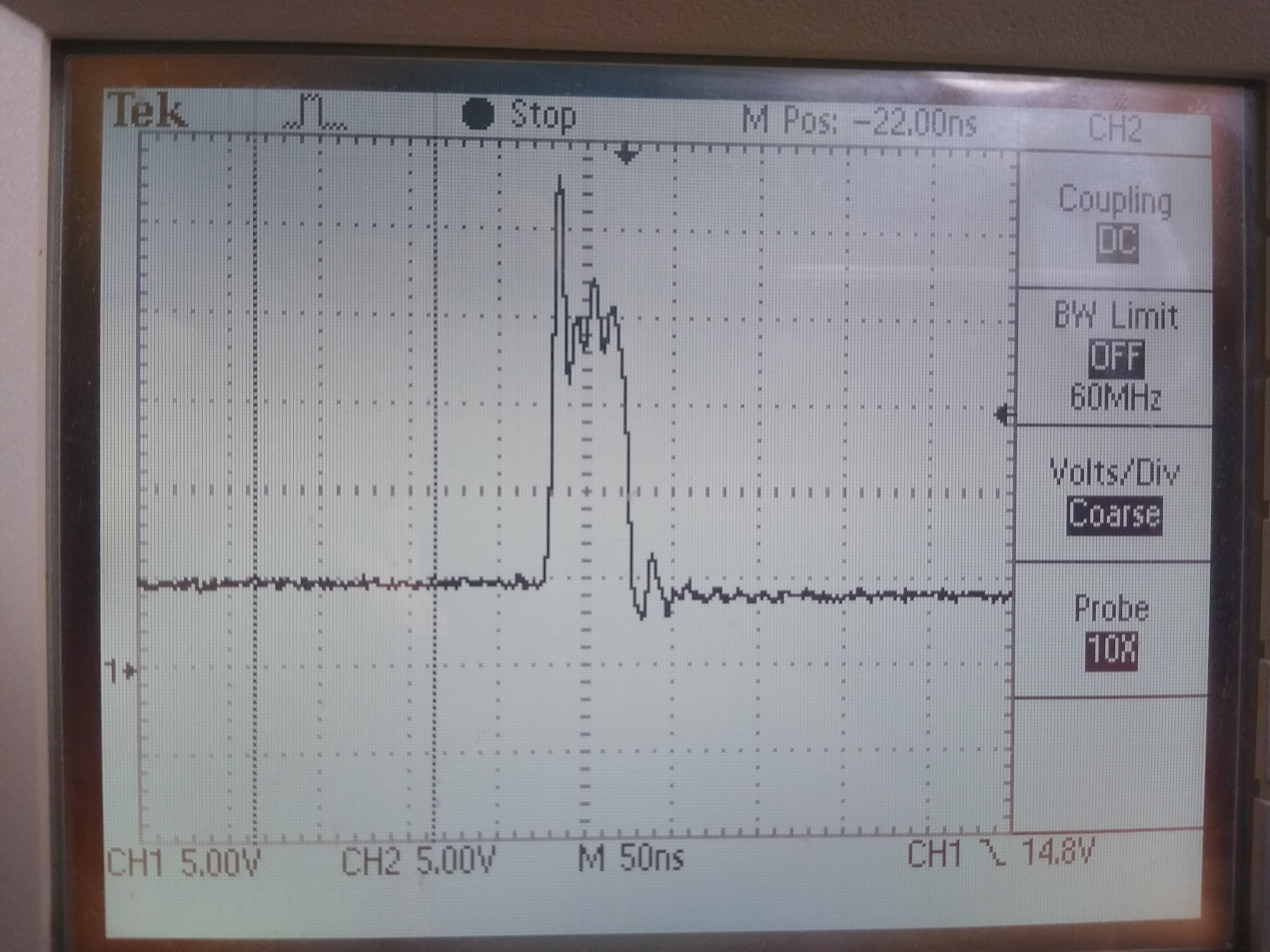
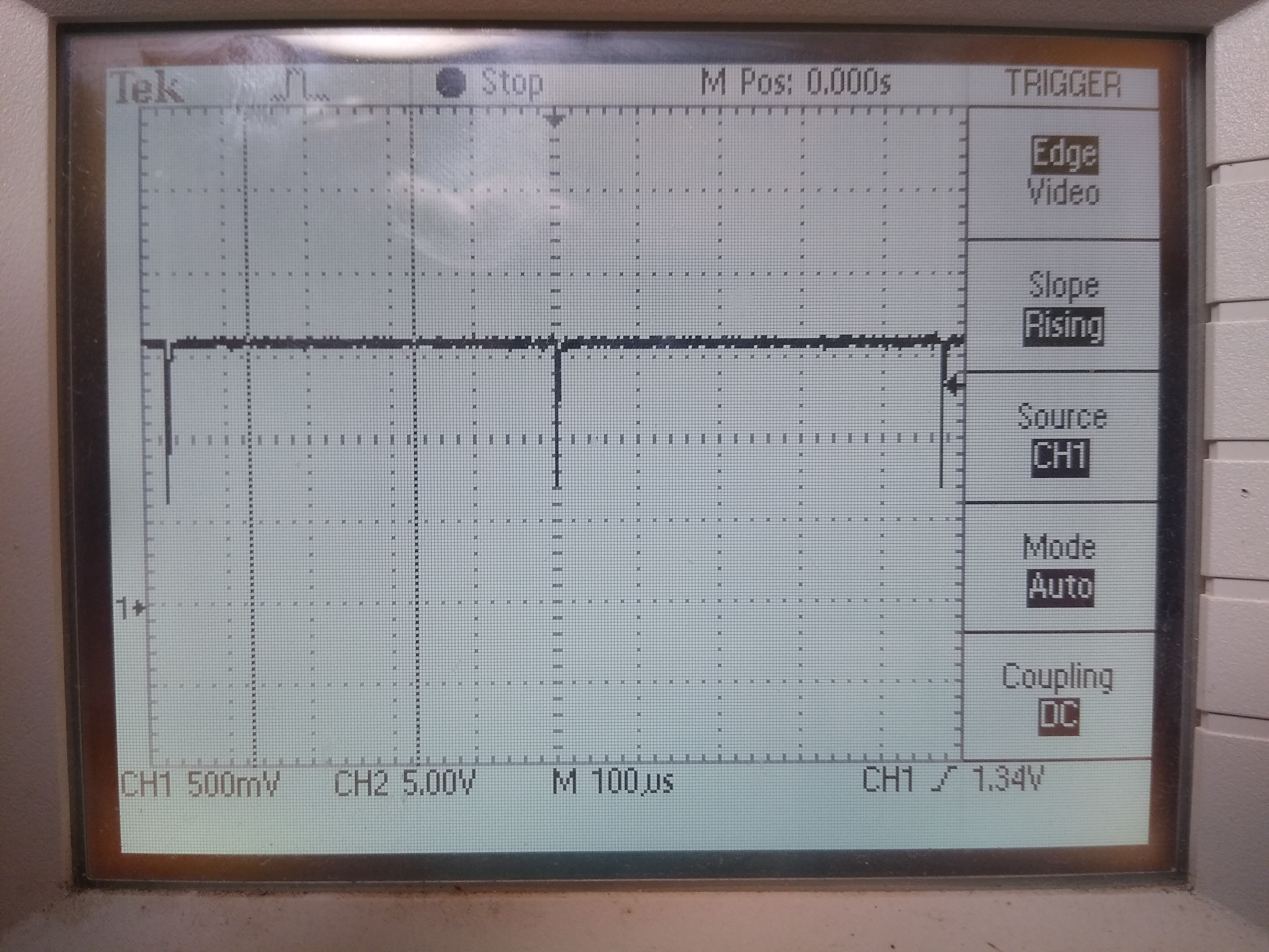
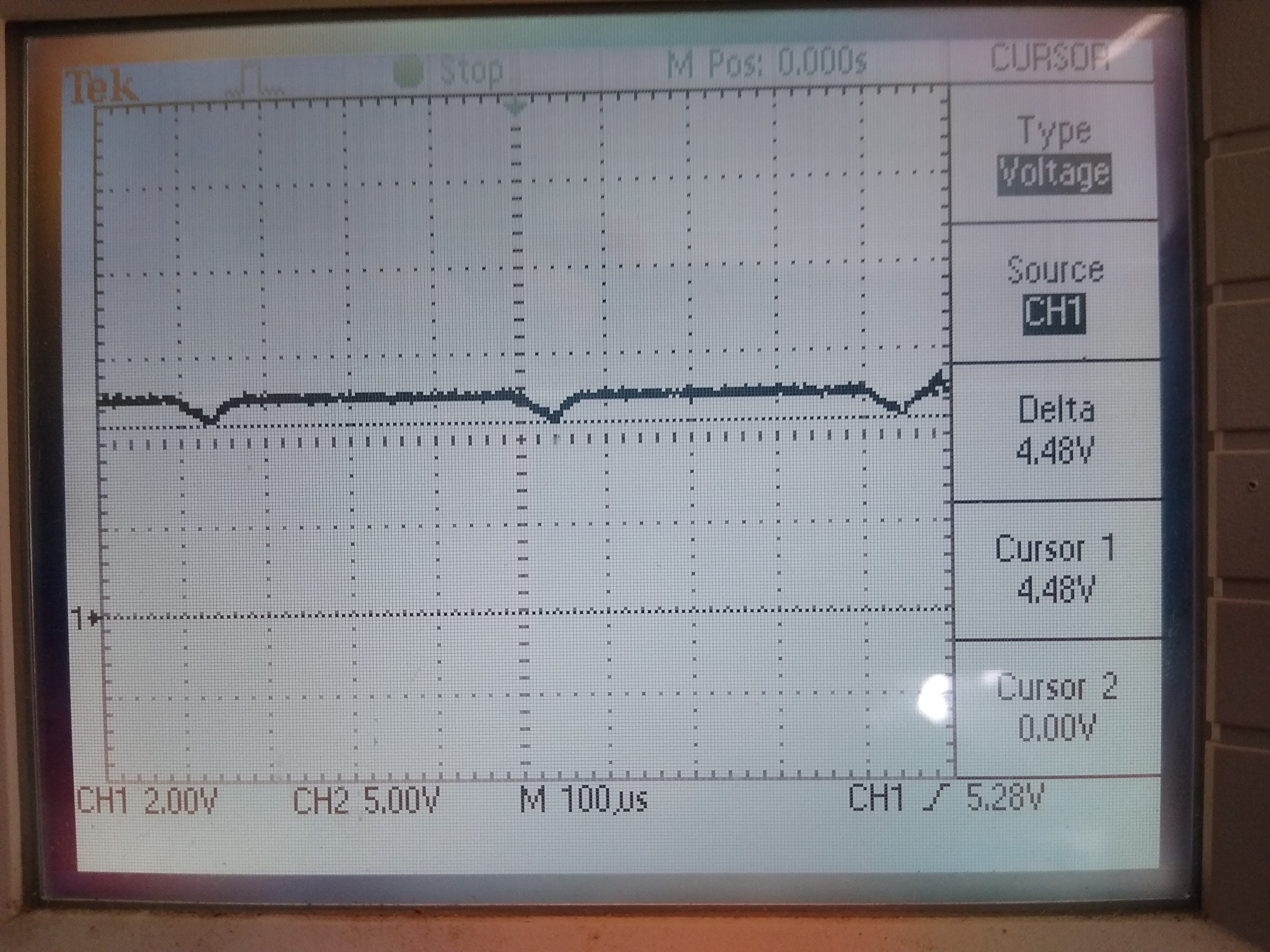
I have looked at all of the voltages on the board an all look correct, but the device doesn't switch - there is very low - no output (0.07V)

DC Voltages measured at nets names on attached schematic:

VIN: 12.0VDC

EN: 1.3V

TRIP: 0.4V

MODE: 0.12V

PGOOD: 0V

VREG: 5.0V

VBOOST: 5.0V

L1: 0.07V

VOUT: 0.07V

VFB: 0.014

What am I doing wrong? Thanks!

2301-101-A_5V_switching_regulator_schematic.PDF

  •  

    The first thing that jumps out is that the EN pin's threshold in the datasheet is 1.3V typical with a range of 1.0 - 1.6V, so 1.3V on the EN pin in your measurements might not be enough to turn the part on.  I would suggest that you start by trying to drive the EN pin to a higher voltage and see if that turns the part on.

    With the enable pin's tolerance range - more then +/- 20%, I would not recommend using the Enable pin as a programmable UVLO with a resistor divider as you have done with R1 and R2 in your schematic.  The existing divider you have could require a VIN voltage of 14.2V to enable the part.

    If you want to use R1 and R2 to implement a course UVLO, you will want to reduce the divider ratio to provide 1.6V on the EN pin when VIN is at the minimum turn-on voltage, but understand that the minimum threshold for this UVLO will be about 63% of the maximum, so there will be a wide range of thresholds with this method.

  • I increased the input voltage to 20V so that the EN pin went up to 2.24V - definitely enabled. The output doesn't switch on. Voltages measured:

    VIN: 20V

    EN: 2.24V

    VOUT: 0.14V

    The enable seems to be working in that if I change the input voltage I get the following outputs:

    VIN: 10.3V / VOUT: 0.0V (really off)

    VIN: 12.0V / VOUT: 0.07V

    VIN: 20.0V / VOUT: 0.14V

    Any other ideas as to what could stopping the part from starting? Thanks!

  •  

    Do you have an oscilloscope to see if the converter is attempting to start-up and failing, resulting in a very low average voltage, or not starting up at all?

    Is the only capacitance on the output the single 33uF output capacitor?  I am wondering if the output voltage ripple coupled with the 40mV of ripple injection from the RCC network across the inductor is causing the circuit to trigger an OV or UV fault, presenting a low average voltage on the SW or VOUT node even though it is attempting to start-up.

    If you can add some additional output capacitance and change R7 from 1.43kOhms to 3.01kOhms we can evaluate if that is the issue. 

  • I checked the voltage at L1 on a scope and it is switching: It is doing a 12V pulse that decays to 0V over 2.5uS, every 400uS. It is as though it is enabling, and then disabling almost immediately, and then retrying in 400uS.

    A the VOUT net, there is no signal. I pulled L1 from VOUT and looked at the coil there and see the 2.5uS pulse when it is disconnected.

    With the coil connected, to insure there is no short on the output, I powered the output with 5V and saw no current draw on the power supply.

  •  

    There are a couple of possible reasons why you might see A single on-time pulse on the input.

    1) D-CAP mode control is designed to operate at very lot frequency when there I no load by emulating a diode with the low-side FET.  This reduces power dissipation and improves efficiency, but normally the converter would trigger a new on-time each time the FB voltage dropped below the 600mV reference, so that does not appear to be the issue here.

    2) The converter is detecting current limit because the drop across the low-side FET is larger than the scaled version of the TRIP voltage, extending the off-time until the drop decreases.  Again, that does not appear to be the issue here.

    3) Turning on the high-side FET is discharging either VIN or EN below their thresholds, shutting down the converter and forcing a restart.

    Can you look more closely at the SW waveform?  If the converter is working correctly you should see a fast, single digit nano-second rise time, an On-time of a few hundred nano-seconds, then a fast, single-digit fall-time back to 0V as the low-side FET turns on.  The could be followed by the low-side FET turning off, leading to ringing on the SW node until it decays back to 0V.  It should not rise up to VIN quickly and then just slowly decay back to GND over 2.5us unless the Boot-strap capacitor (SW to BOOT) is missing, damaged, or undersized.

    Check the voltage on the BOOT pin, it should be charged to VREG when the SW voltage is low, and then track the SW voltage up when the SW voltage pulse high using the voltage stored on the BOOT capacitor.

    Also check the EN and VIN pins to make sure they are not dropping when the high-side FET turns on and draws current out of the VIN bypass capacitors.  If there is too much resistance or inductance between input bypass capacitors and the VIN pins, VIN or Enable could be dropping out and triggering a shutdown of the output voltage.

  • This is the waveform I get with VIN range of 13.3-15.7V (EN=1.24-1.70V). I'm still checking the other signals you suggested.

  • Here are screen shots of the other signals (top trace: VL1, bottom trace: TRIP / MODE / ENABLE / 

    Trip:

    Mode:

    Enable:

    VIN Note that this noise was seen on VREG too:

  • Here are the other signals vs VL1:

    Enable:

    Mode:

    Trip:

    VIN: (note that VREG reflected this noise on VIN, but did not drop much - 0.1V)

  • I took scope traces of the other signals you requested:

    Trip:

    Mode:

    Enable:

    Vin: (the small ripple on VIN is reflected on VREG)

  • My guess is that it is the enable line because it is getting pulled low somehow. Here is a zoomed out shot it. It's getting clobbered every 460uS by something. What would cause this to drop? It is only an input; is there something internal to the chip that could affect this?

    ENA:

  • I pulled the inductor off and still see the same SW waveform. I don't understand what this indicates.

  • I got some better scope shots.

    VSW, Toff =  400uS.

    VEN, Goes low every 400uS:

    VBOOST looks okay:

    MODE:

    TRIP:

  • Have you had a chance to look at my latest post. I have better scope shots.

    They show that the regulator is switching, but only ever 400uS. The EN goes low then too, which I do not understand because it's an input.

    Any help would be appreciated. Thanks!

  •  

    The waveforms indicate that the Enable voltage is getting pulled down low enough to disable the converter with each switching cycle.  That's why we see it switching once every 460us, it gets enabled, but on the On-time the part gets disabled, shutsdown and then has to restart, waiting another 460us to generate a new On-time.

    The only thing in the Enable pin that could draw current into the part, unless the part is damaged, would be the internal pull-up back to VREG.  If VREG is lower than Enable, the Enable pin could sink current to the VREG pin.  It would be worthwhile to check to see if VREG is getting discharged along with Enable and double check the VREG bypass capacitor.

    You could also try adding a 0.1uF bypass capacitor to Enable across the bottom resistor.  That might provide some additional insight into why Enable is dropping out.

  • I measured VREG and it is dipping every 460uS, but only to 4.45V. It should not be dipping at all though, should it?

    I added a bypass cap across the lower ENDIV voltage divider and the output went from 0.03V to 0.3V.

    Should the enable voltage divider have a lower resistance? Seems like 681K / 86.8K is very high.

  •  

    Vreg will get discharged when the converter switches as the gate drivers draw pulses of current from the Vreg bypass capacitor, so that's not unexpected, but that drop shouldn't be enough to trigger a UVLO.

    Yes, let's try reducing the enable driver by reducing both enable resistor by a factor of 10, the increase in VOUT is likely a result of the converter switching longer between shutdowns with the longer time-constant for the enable voltage, holding the enable voltage up longer during each discharge.

  • I take it reducing the impedance of the Enable driver solved the problem?

  • No. It still didn't work. I had to find another solution from another vendor. Out of time.