This thread has been locked.

If you have a related question, please click the "Ask a related question" button in the top right corner. The newly created question will be automatically linked to this question.

UCC28630: Output overvoltage during startup with spikes in CS signal

Part Number: UCC28630
Other Parts Discussed in Thread: UCC28704

I have a design based on the example in the datasheet, but regulated for 5v output, however I cannot get it to start as the circuit during the exploratory three pulses goes into overvoltage on the output.

I have reviewed the design process and cannot find any glaring issues, however I did find a weird signal on the CS pin.

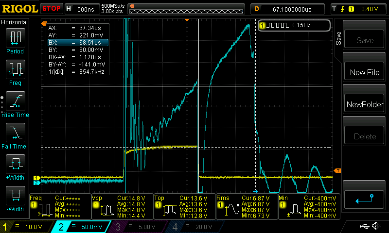
Channel 1 is the DRV output to the MOSFET and channel 2 is measured on the top of R_CS.

After the exploartory pulses the SD pin signals output overvoltage (as found in another post) and this is very well in line with the output being built up to > 6 v at this time.

  • Hello,

    The UCC28630 during power will give three pulses.  If there is not a fault present the converter will start to switch.

    The faults are

    1. Input under voltage
    2. Output Over Voltage
    3. Input over current

    When a fault is seen switching stops and VDD will cycle between VDD(start) and VDD (stop).

    There is an application not at the following link that will give you some guidance on trouble shooting the design that you might find useful.


    Please note that an OVP can be triggered at any point after the gate drive goes low and Vo sample delay.  Please refer to figure 25 in the data sheet.  It is also recommended that their be less then 100 mV of ripple on the aux winding at the sample point.

    Your transformer leakage inductance needs to be less then 3% of the magnetizing inductance.  Excessive ringing can be reduced with a snubber on the output rectifier and setting up and RCD clamp on the switch node.

    We also have a lot of 5V PSR fly back designs.  The following link will get you to a 10 W PSR flyback design using the UCC28704 with a 5 V output that you might find interesting.


    Their is also an Excel and Mathcad design tool that you might find helpful.  They are the same calculations that are presented in the data sheet.  You can find them a the following link. https://www.ti.com/product/UCC28630?keyMatch=UCC28630&tisearch=Search-EN-everything&usecase=part-number#design-development

    We have many reference designs for many applications that can help you get started with your design as well.  They will give you Gerber files for the layout, a bill of materials and test report.  You just need to enter your input and output power requirements and the reference design we have already that come close to meeting  your needs will show up.  You can find these designs at the following link.

    Regards,