This thread has been locked.

If you have a related question, please click the "Ask a related question" button in the top right corner. The newly created question will be automatically linked to this question.

BQ76952: How to calculate these resistors(black circles) values around CHG NMOS and DSG NMOS

Part Number: BQ76952

Hi team,

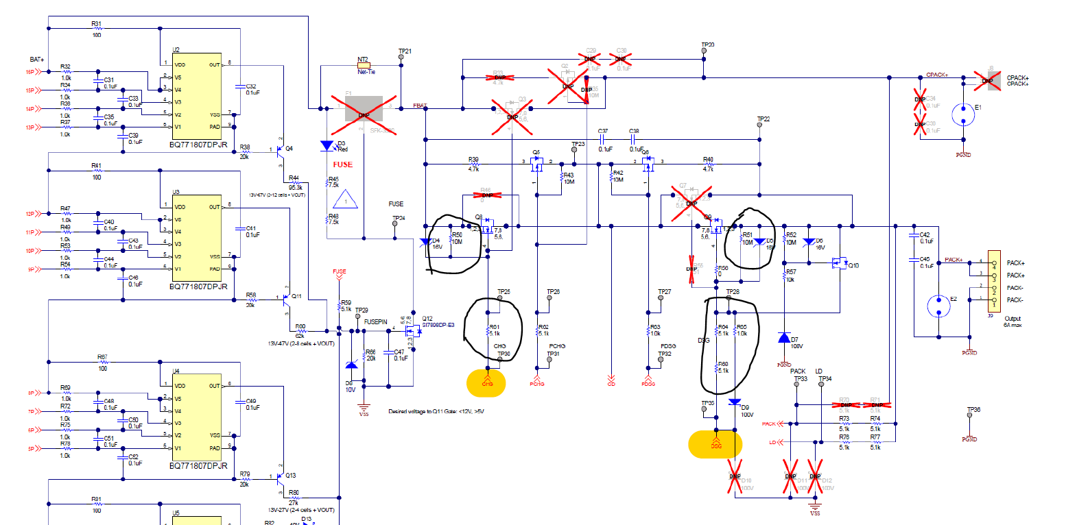
Nice to see you by email. When looking through datasheet of BQ76952, there are some parameters of High-side NFET Drivers. My question is how to calculate these resistors(black circles) values around CHG NMOS and DSG NMOS? Can you share detailed method of calculating these resistors?

thanks and best regards,

Sophia

  • Hi Sophia,

    For some reasons the images are not showing in your post. Maybe you can try to insert them again.

    The gate resistors for the FETs should be around 5k ohms. A lower value can help with faster turn-off for the DSG FET, but too fast turn-off may have higher risk of damage during a short-circuit event. There will be more guidance in the final production datasheet for selecting these values.

    Best regards,

    Matt

  • Hi Matt,

    The image is as below. Can you share some data about capability(current) of high-side driver with me by email? Because I can calculate rise and off time with different NMOS and Rg based on driver current. By the way, how to select Rgs?

    thanks and best regards,

    Sophia

  • Hi Sophia,

    The charge pump can only provide limited current.  To estimate its capability look at the start up time and calculate from the CP1 capacitor value, I=CdV/dt.  With the data sheet values you get about 50 uA. Also remember that charge pumps have an efficiency requiring more current in than they produce. So you want to keep the Rgs resistors large, the 10M is suggested for a load of about 2.2 uA.  Turn on of the FETs is from the charge stored in the CP1 capacitor, the charge pump will replenish the charge over time.  The drivers do not have a under voltage cut off, so if the FET load is dropping the capacitor significantly a larger capacitor can be used, it will take longer to charge initially and to recover.

    The data sheet shows the test conditions for a gate resistor of 100 ohm.  The driver specification does not provide a resistance.  The system engineers expect the user to calculate the effective resistance from the data sheet rise and fall time and calculate time with the new load.

    The charge driver is driven more slowly as shown in the data sheet.  With its limited range a smaller value could be used.  For a single FET the 5.1k mentioned and shown in the EVM schematic is a good value. Generally with more FET gate capacitance the resistor would be made smaller.

    The discharge FET driver has a larger range.  With a reverse charge situation the discharge FET will be pulled the system voltage below GND while the DSG output pin can and will not go below GND.  Since the BQ76952 can not drive the gate in this condition the external clamp FET shown holds the gate to the source. The gate resistor must be selected with the resistance and power rating to dissipate the heat generated during the reverse charge duration. That will often be a large value.  The topology shown in the schematic with the Schottky diode allows a faster turn off with a smaller resistor.  Turn off of the DSG can be very quick with a 100 ohm resistor, but this can excite cell inductance to create a large transient.  Adjusting the resistor value in the 5 k to 7.5 k effective resistance range will often control the switching speed to avoid a large spike with a single FET.  With larger FET Ciss or more FETs the resistance should be made smaller. 100 ohm is a recommended minimum value to limit current in the IC pins.

    When using small resistors to achieve a fast switching time be sure to use suitable techniques in the system to suppress an inductive transient before it reaches the IC.