This thread has been locked.

If you have a related question, please click the "Ask a related question" button in the top right corner. The newly created question will be automatically linked to this question.

TPS22913: Asking for the design question on TPS22913

Part Number: TPS22913

Hi Team,

Customer is designing TPS22913.

Would you please provide comment for the following questions?

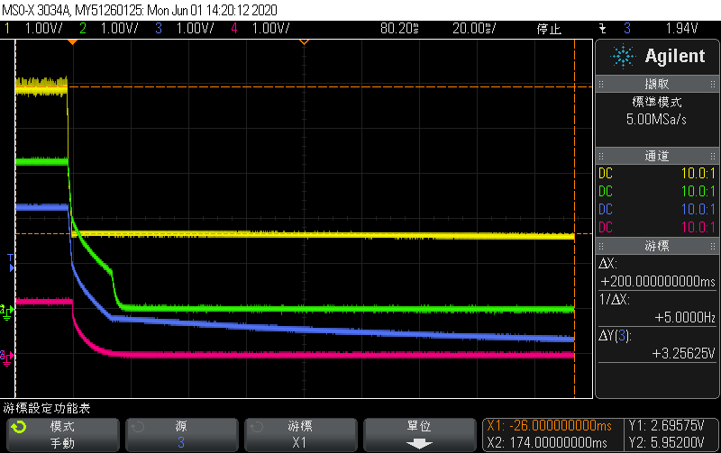
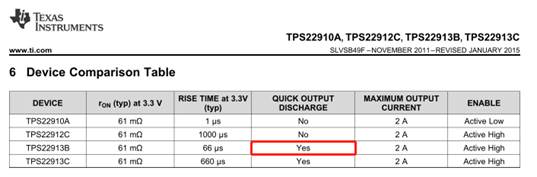
Q1: In TPS22913B d/s, TPS22913B has the quick discharge function.

However, customer found the output 3.3V drop slowly after power off. How to verify this quick discharge function?

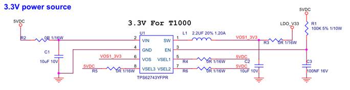
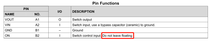
Q2:customer uses T1000 IC’s GPIO to control TPS22913B ON pin. (B2).

And customer change R23 to and capacitor due to customer use R23(capacitor) and R22 as RC delay.

There is short period that TPS22913’s ON stay at “floating” during power up stage until T1000 send the enable signals.

Is that acceptable?


BR,

SHH


  • Hi SHH,

    Welcome to E2E!

    The TPS22913B does have a QOD discharge function when the device is disabled.

    What is the total fall time of the output?

    What is the output capacitance in the circuit?

    How much current is being supplied to the load?

    I am not sure which R23 and R24 components you are referring too, but the ON-pin should not be left floating. To make a proper RC delay the customer could create a voltage divider circuit on the ON-pin with a resistor paralleled to the capacitor and the TPS22913. This will keep the ON-pin from floating when there is not signal being applied to the ON-pin.

    Best regards,

    Andy Robles

  • Hi Andy,
    Please refer to the update schematic here.

    BR,
    SHH

  • Hi SHH,

    The customer may change R23 to a capacitor and place a resistance on R22(not 0 ohms) to create an RC delay for the TPS22913B. The ON-pin should still not be left floating. If the signal CHIP_EN is able to send a 0V/LOW/GND signal to ON-pin then disabled then you wouldn't need add additional components. If the CHIP_EN signal is left floating when disabled, then you will have to add a resistor in parallel to R23(i.e. resistor connected from ON-pin to GND) to keep the ON-pin from floating when the device is disabled.

    Best regards,

    Andy Robles

  • Hi Andy,

    thanks for feedback.

    What is the total fall time of the output? it is over 160ms. the blue line is the output voltage

    What is the output capacitance in the circuit? C16 100nF

    How much current is being supplied to the load? customer is unable to measure this current. What do you want to do for this current measurement.

    TPS22913B should has discharge function. Would you please provide comment why the output voltage discharge slowly?

    BR,

    SHH

  • Hi Shh,

    Does VIN also ramp down at the same time the switch is disabled?

    Would you be able to get a scope shot with the signals on VIN, VOUT, and ON-pin of the load switch?

    Best regards,

    Andy Robles