Hi everyone,
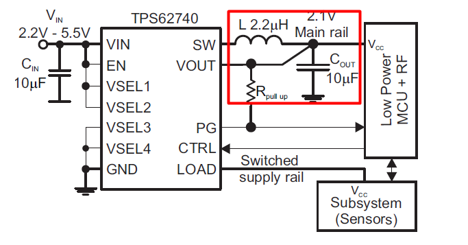
I will use the TPS62740 in one of my designs. I will utilize the LOAD pin to supply some of the analog and digital components such as Voltage reference, Op Amp, Multiplexer, Flah memory etc.
So I have to use both AVdd and DVdd lines. I will split the LOAD pin output to create these voltage rails as shown below
My questions are:
1. Is this approach correct for creating AVdd and DVdd?
2. I have to decouple both legs or could I decouple right next the LOAD pin? Should I use the same RL filter provided at the datasheet (decoupling the Vout)?
Thanks in advance
Nick


