This thread has been locked.

If you have a related question, please click the "Ask a related question" button in the top right corner. The newly created question will be automatically linked to this question.

TPS22914: delay time on external voltage applied

Part Number: TPS22914
Other Parts Discussed in Thread: TPS2115A, LM66100

Hi, team

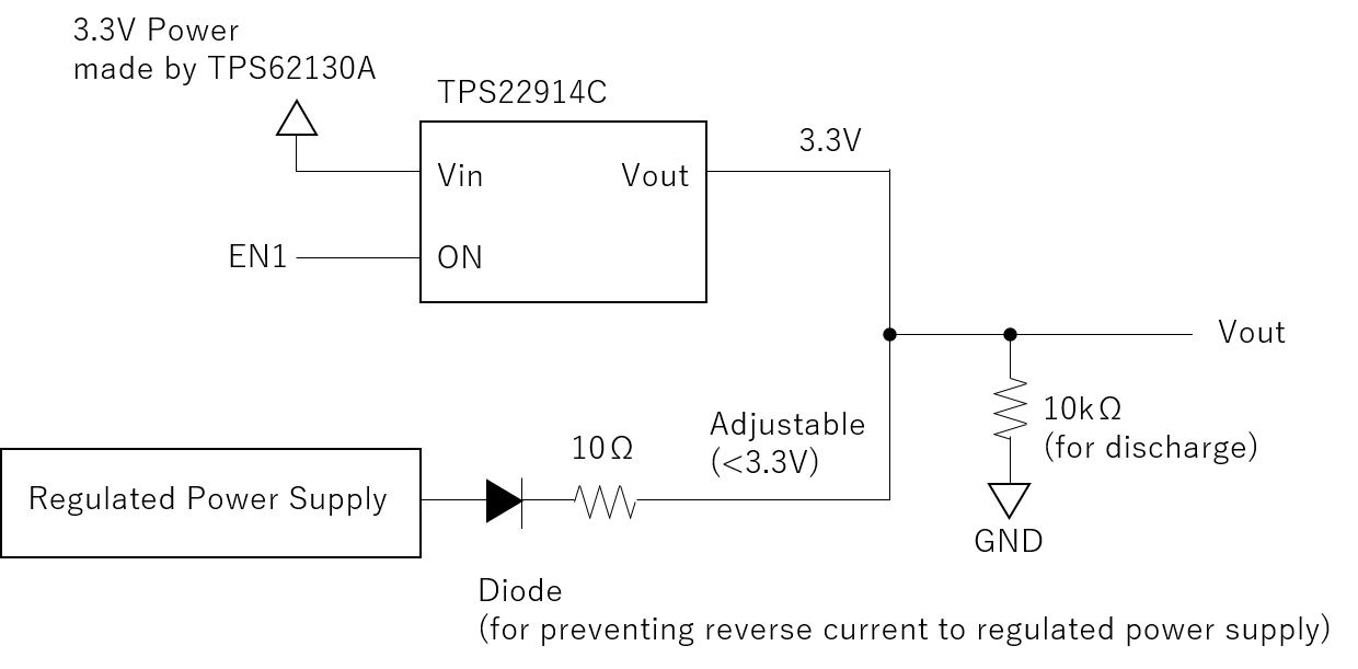
I designed Power MUX using TPS22914C and TLV74218P as below.

In measurement, delay time was 1.8ms when rising 1.8 to 3.3V.

In datasheet of TPS22914C, delay time is 913us (typ).

In the case external voltage applied, is there the factor delay time extend? 

Best regards,

Naoki

  • Hi Naoki,

    I see in your scope capture the EN is going low. TPS22914 is an active high device so I think this is EN_1.8V? 

    Can you please recapture this issue while probing VIN, VON and VOUT of the TPS22914C?

    For reference, the typ rise time for TPS22914C is 913us and the typ delay time is 622us at 3.3V.

    Finally, for dedicated powerMUX applications is it possible to use TPS2115A in your system instead?

  • Hi,

    Sorry,I recapture probing VIN, VOUT, VON of TPS22914C. and VON of TLV74218P.

    delay time is about 1.8ms and this is apart from 913μs.

    In the case external voltage applied, is there the factor delay time extend? 

    Extension of delay time is not problem but I need to know max delay time.

    I cannot use TPS2115A because of the drop while voltage switching.

    Best regards,

    Naoki

  • Hi Naoki,

    Thank you for providing the scope capture. I wanted to be certain before giving an answer.

    When putting an external voltage on the Vout, the timing of TPS22914C is affected and it can be longer than the datasheet specification. TI does not spec the timing of load switches with voltage on the VOUT pin and so those values may not hold.

    As a result, I cannot provide a "max delay time" for this use case. Do make-before-break OR-ing topologies like LM66100 work better for your solution?


  • Hi,

    If putting an external voltage on the Vout, Charge Pump and Control Logic is connected external voltage through body diode as below block diagram.

    However, Vin =3.3V is already exists and it is higher than an external voltage. So, I cannnot understand the reason why the timing of TPS22914C is affected.

    Gate drive circuits watch Vout ?

    If so, I can understand the difference of gate drive with an external voltage exisit or not.

    Best regars,

    Naoki

  • Hi Naoki,

    When an external voltage is placed on the output, internal references to control blocks within the device can be affected. This is not necessarily due to back conduction through the body diode since VIN=3.3V as you rightly mentioned. The timing data on the datasheet (for this device) is specified in a way that does not involve external voltage on VOUT. TI does not spec this parameter. If the internal references are shifted, then the timing could deviate from what is on the datasheet.

    I suspect that the timing might also be affected due to the make-before-break system you are using. Usually, MUX-ing with load switches is meant to be a break-before-make topology. If necessary, the test could be run again but with turning off the TLV74218P before turning on the TPS22914.

  • Hi,

    Changing external voltage on the output, the following results were obtained.

    Delay time is proportional to external voltage.

    From this result, can be maximum delay time estimated roughly ?

    I want to estimate maximum delay time from 1.8 to 3.3V.

    Delay time from 1.8V to 3.3V can be longer than one from 2.5V to 3.3V ?

    Best regards,

    Naoki

  • Hi Naoki,

    Do you have an EVM to perform testing on the TPS22914C? Is this repeatable over multiple devices in your system?

    I may not be able to provide exact timing data but I will try to confirm the device behavior. If possible, I will perform inhouse testing and get back to you tomorrow with and update. If you would like, we can take this thread to direct email support. Please email me at s-dmello@ti.com and feel free to send any relevant data from your system.

    Thanks for choosing TI Power Switches in your designs.


  • Hi,

    At previous post, I evaluated using TPS22914C and Regulated Power Supply.

    I don't need exact timing data.

    I want to grasp maximum delay time from 1.8V to 3.3V roughly.

    I would appreciate if you confirm the device behavior.

    Best regards,

    Naoki

  • Hi Naoki,

    In this test you are turning on the TPS22914C into a pre-charged rail that is being actively supplied by another source. The device is meant to switch a passive load and not to an active rail. As such it is difficult to provide any confirmation here.

    Can you re-do the test once more with a 10 Ohm resistance in series with the diode (from the diode to Vout) ? 

  • Hi,

    Thank you for your comment.

    I re-tested below block diagram.

    As a result, the tendency of proportional of external voltage is no change.

    Best regards,

    Naoki

  • Hi Naoki,

    Thank you for helping us out with this test. On our end we performed in-house simulations. Thank you for also re-doing the test with small differences as it has helped us expedite this request.

    The extended delay timing is expected behavior of the turn on of the device. With more charge on the Vout, the delay will be extended longer. This is due to the turn on physics of the integrated NFET.

    As I mentioned before, I cannot provide exact timing details but a direct relation that you are seeing is expected. When no charge is placed on the output, the datasheet specification will hold. 

    Thank you for choosing TI Power Switches in your designs.

  • Hi,

    Thank you for performing in-house simulations.

    How does the integrated FET affect the behavior of turn on ? Charging time of reference voltage become slower and turn on time extends ?

    To estimate maximum time, I want to know the principle of the turn-on behavior roughly. 

    I intend to estimate maximum delay time when transition from 1.8V to 3.3V based on the measured data.

    So, I want to know variation to some extent. 

    The measured data (2.5V →3.3V) can be used as maximum time when transition from 1.8V to 3.3V ? Or additional variation should be considered ?

    Best regards,

    Naoki

  • Hi Naoki,

    As mentioned, it is not possible to provide details on timing apart from the general behavior in this case. This is not recommended operation.

    For an NMOS, the channel is formed when Vgs>Vth. As Vs is increased and precharged, charging of the gate is lengthened.

    Thank you.