This thread has been locked.

If you have a related question, please click the "Ask a related question" button in the top right corner. The newly created question will be automatically linked to this question.

WEBENCH® Tools/TPS610985: Suggested layout of WEBENCH - how reliable?

Part Number: TPS610985

Tool/software: WEBENCH® Design Tools

Hi,

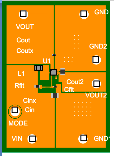
how reliable are the suggested layouts of webench?

As far as I know it's very important to place inductor and input/output caps very close to the IC.  All that's not the case buy the suggested solution. Also there is a big copper trace between L1 and the IC. Isn't that usually very critcal?

Can anybody explain that layout and behaviour of WEBENCH?

  • Hello Makes,

    The layout in Webench is based on the EVM layout, but optimized for the use with different external component sizes. E.g. the trace you can see above for the inductor is caused by the ability to place smaller and bigger inductors. The one in your design is smaller and therefore the layout of the trace looks somewhat strange.

    The Webench layout is functional, but might show a slightly worse performance than the EVM layout.

    Best is to stick as close as possible to the EVM layout.