


Hi Experts,
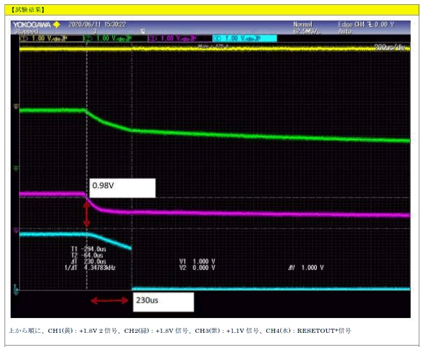
My customer is evaluating the propagation delay of voltage detector comparator. The spec is defined as below.
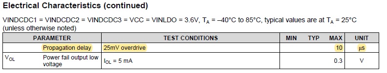
Customer connects PWRFAIL_SNS pin to L1 pin(1.1V). When power on and power off, this propagation delay is much longer than 10us.
Power ON:
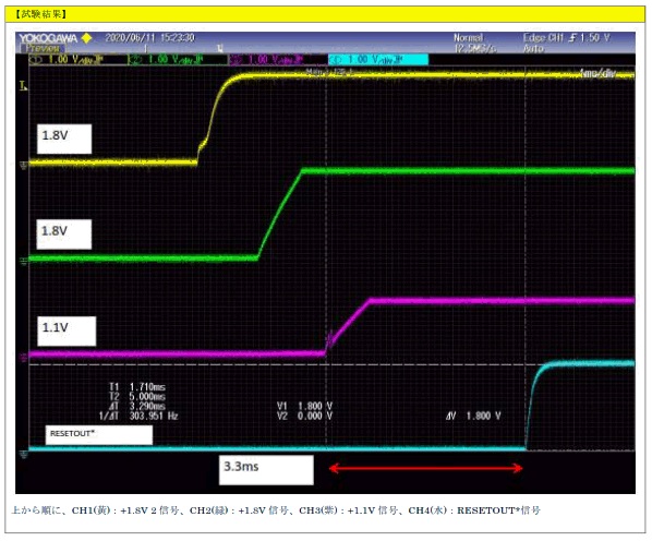
POWER OFF:
Are these the expected behavior?
Regards,
Hisao Uchikoshi
