This thread has been locked.

If you have a related question, please click the "Ask a related question" button in the top right corner. The newly created question will be automatically linked to this question.

TPS544C25: The power output is strange. Is there something wrong with the circuit?(TPS544C25RVFT)

Part Number: TPS544C25

Hello

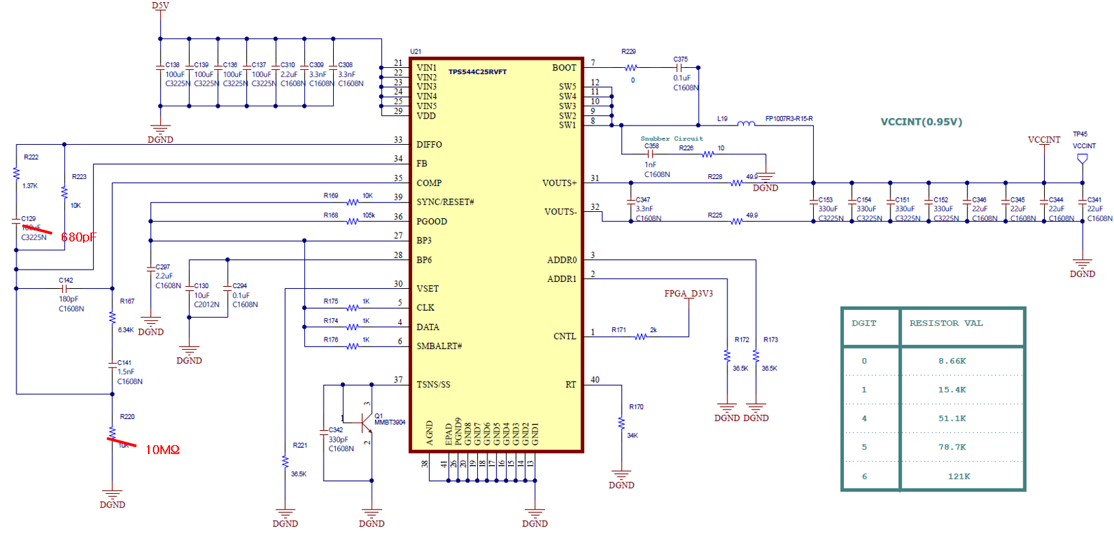
I am using a TPS544C25RVFT regulator, but the power output is strange.

Looking at the capture screen, a square wave is output based on 0.95V.

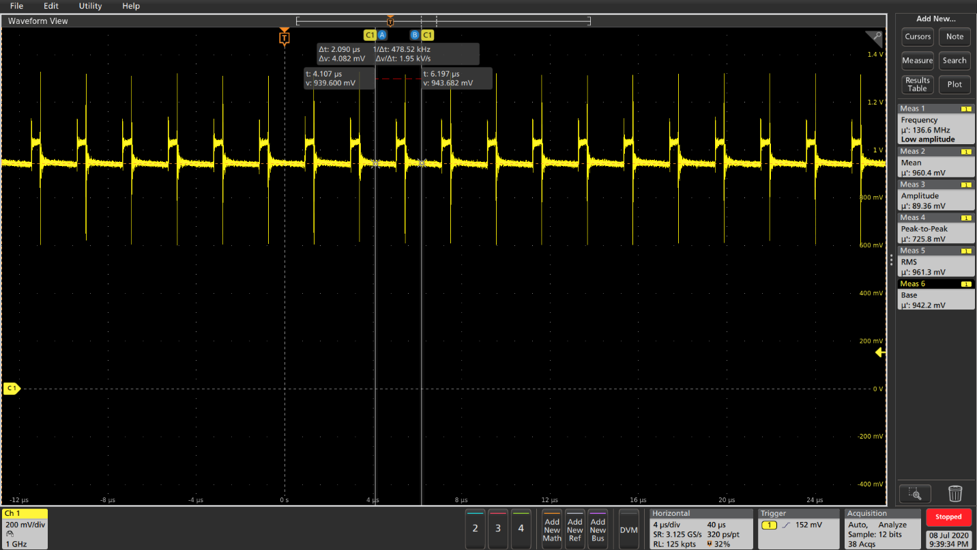
Shouldn't 0.95v be output linearly?

The circuit is designed like a capture screen.

Please let me know if there is something I am missing

  • Hi, seems switching noise coupled, could you please confirm it is not related to the measurement method? use 20Mhz bandwidth and shortest probe GND line, and test probe far away from switching node.

    https://e2e.ti.com/blogs_/b/powerhouse/archive/2016/07/27/how-you-measure-your-ripple-can-make-you-or-break-you

    Yuchang

  •  

    Yes, it appears that your oscilloscope is picking up switching noise from the switch-node, or the ground reference for the probe is moving with the switch node.

    Some things to look out for:

    1) Two ground clips connected to the same board at different places

        Oscilloscope probes use a common ground bus at the oscilloscope input, which is often connected to earth ground, if 2 ground clips are connected at different points, they oscilloscope will amplify the difference between these ground points by 5x, negatively affecting the measurement accuracy as the voltage difference between the grounds is forced on the ground wires of the oscilloscope probes, then scaled up by 10x to counter the 10:1 attenuation of the passive probes.

    2) Pick-up from the switching node.

    A passive probe with a long ground lead that forms a loop near the inductor of a switch mode power supply can form an air-core transformer with the inductor, imparting a scaled down version of the switch-node voltage on the oscilloscope measurement.

    If you have eliminated multiple ground connections and long ground leads, it is possible that the square-wave pattern is really on the output.  The square-wave would represent the inductive portion of the output ripple, but the level seen is quite high, so the parasitic layout inductance would be extremely high.  For a 5V input to produce a 90mV square-wave at the output voltage, the parasitic layout inductance would need to be 0.09/5 = 1.8% of the main inductor. 

    For the FP1007R-R15 inductor, that would be 2.7nH parasitic inductance.  If you have checked your oscilloscope measurement and are confident in that, look at the layout and output capacitors.  They should be connected a wide VOUT copper pour and the grounds should be returning to the system ground plane with multiple parallel vias.

  • Hi Shin

        Just checking with you if your issue got resolved.

    Regards,

    Gerold

  • Hi Shin,

        As we have not heard back from you, we are hoping that our answer has helped solve your problem. If you still have further questions on this topic, please type them here.

    Regards,

    Gerold