This thread has been locked.

If you have a related question, please click the "Ask a related question" button in the top right corner. The newly created question will be automatically linked to this question.

TPS62162: Inquiry about occurred short at Vin, SW, GND of this part when power was inserted

Part Number: TPS62162

Hi,

I got an issue from my customer.

Test condition is below.

 -. Vin : 12V

 -. Vout : 3.3V

 -. Average load current : about 350mA

 -. Bypass cap. at Vout : Ceramic Cap. (22uF - 1ea, 10uF - 3ea, 1uF - 3ea), Tantalum Cap. (10uF - 2ea)
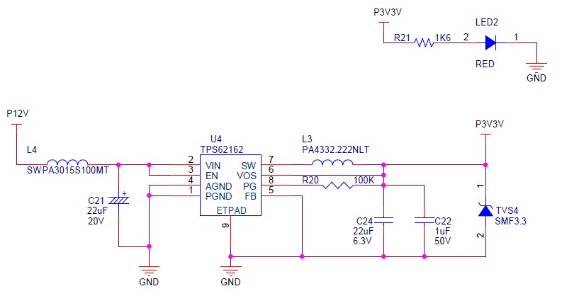
Below is schematic

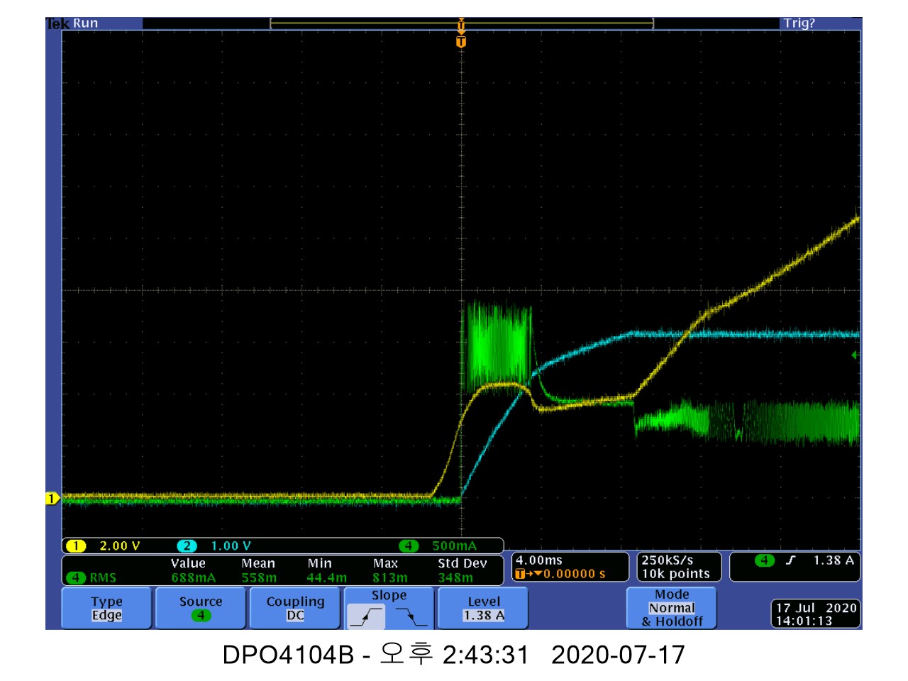
Once power 12V is inserted to tps62162, we can see LED On for very short time.

But, this device is not work again.

When I checked pin status of this device, Vin/SW and GND pins was shorted together.

The number of this issue is 5parts.

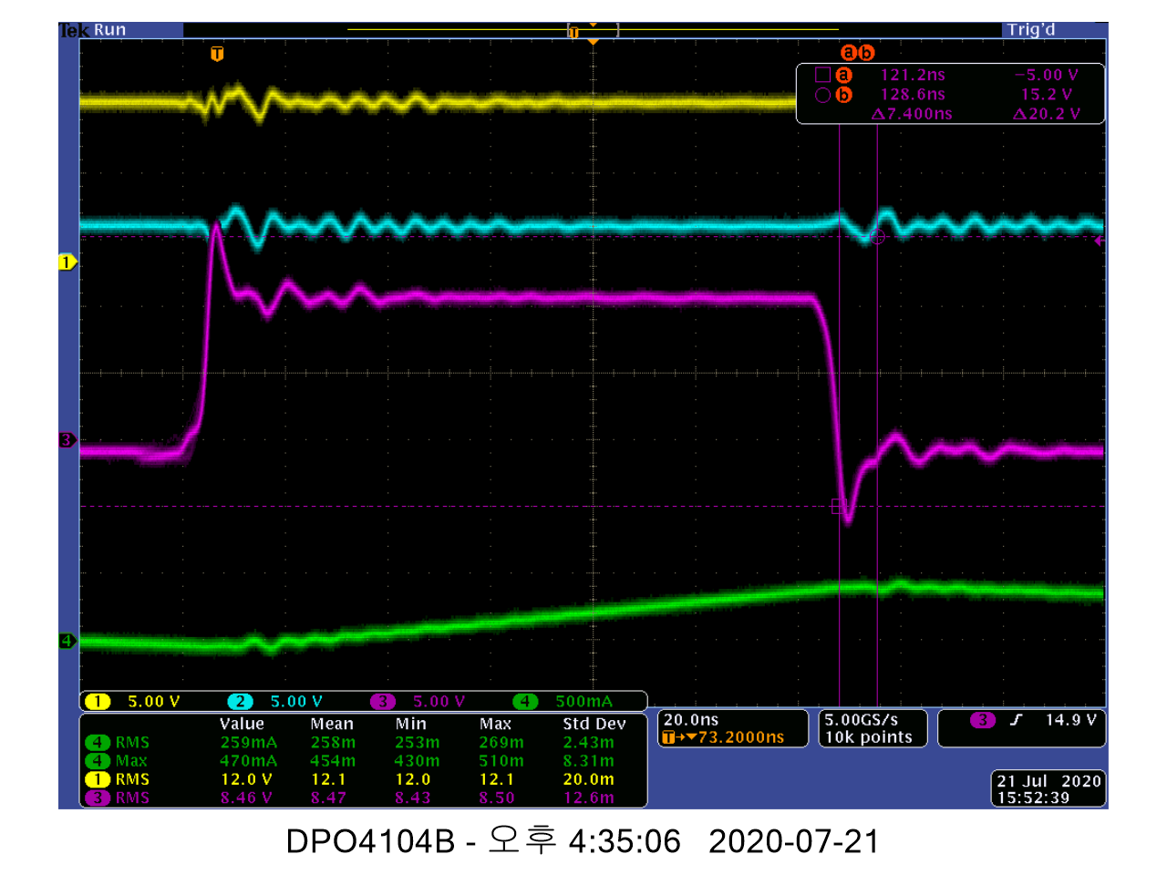
Below is waveform of Vin, Vout, Iout when this device is normal operating.

We can see peak current between 0V and 2V before Vout is reached at 3.3V.

(For your reference, If I remove Tantalum Cap. 10uF on the B'd, peak current is decreased.)

I know that this device has current limit and short circuit protection function.

So, I think that this device does not have to be dead.

But, this issue has happened.

Finally, I need your help and guide about this issue.

1. Give me your overall review and opinion about this issue.

2. Could you explain to me which condition can make damage (Vin/SW and GND was shorted) to this device like this symptoms.

I'm looking forward to receiving your good reply.

Best regards,

Michael

  • Michael,

    Some comments:

    1. I would recommend using just the 1x22uF cap with the 1uF cap at the output. Too much output cap with low soft-start time can cause current limiting issues which seems like the design is running into. This device has internal soft-start time with 50us delay. I expect around 200us ramp up time but the output voltage on your waveform is taking quite long (4ms/div?)

    2. What is the green waveform? Is it IOUT or inductor current? 

    3. Can you share SW node waveforms? EOS on VIN, and SW nodes can cause FET damage which is likely what is happening here. If possible, a failed case and a good case to compare against would be best.

    3. Can you confirm if your VIN supply has no issues - the VIN ramp up is not monotonic.There is an input filter with 10uH inductor with a 22uF cap at the input. Can you confirm the cap C21 part number? I would add a ceramic cap at the input in parallel to C21. This cap can be 10uF or higher as long as it is ceramic. You need to check and see if there is any ringing at the input due to this filter.

    4. I see a TVS at the output - can you give some details on its need?

    5. You mention 5 parts have this issue. How many other designs have you checked that do not have the issue?

    Regards,

    Amod

  • Hi Amod,

    Thanks for your kind and fast support.

    Here is your requested and let me know your final opinion.

    2. What is the green waveform? Is it IOUT or inductor current? 

        [Michael] Iout

    3. Can you share SW node waveforms? 

        [Michael]

        It seems like over/undershoot is too high.

    3. Can you confirm if your VIN supply has no issues - the VIN ramp up is not monotonic.There is an input filter with 10uH inductor with a 22uF cap at the input.

        Can you confirm the cap C21 part number? I would add a ceramic cap at the input in parallel to C21. This cap can be 10uF or higher as long as it is ceramic.

        You need to check and see if there is any ringing at the input due to this filter.

        [Michael]

        Vin Cap.(C21) : 293D226 (Vishay)

        293D SERIES.pdf


        12Vin waveform (Yellow)


    4. I see a TVS at the output - can you give some details on its need?

        [Michael]

        When I visited our customer at first, They said that TVS Diode is not a problem.

        But, I think that TVS Diode spec. will be root cause of this issue.

        I need your detail opinion.

       Littelfuse_TVS_Diode_SMF3_3_Datasheet.pdf.pdf

  • Hi Amod,

    I replied to you but it looks like posted at any of the website.

    Anyway, thanks for your kind and fast support.

    Here is my reply what you requested.

    2. What is the green waveform? Is it IOUT or inductor current? 

       [Michael] Iout

    3. Can you share SW node waveforms?

       [Michael]

       Ch3 is SW.

       It looks like Over/Undershoot is too high.


    4. Can you confirm if your VIN supply has no issues - the VIN ramp up is not monotonic.There is an input filter with 10uH inductor with a 22uF cap at the input. Can you confirm the cap C21 part number? I would add a ceramic cap at the input in parallel to C21. This cap can be 10uF or higher as long as it is ceramic. You need to check and see if there is any ringing at the input due to this filter.

       [Michael]

       12Vin is Yellow.

       C21 is 293D226 (Vishay)

       2311.293D SERIES.pdf

    5. I see a TVS at the output - can you give some details on its need?

       [Michael]

       When I first visited our customer, they said that TVS diode spec. is not a problem.

       But, at this time, I think that there is no room at breakdown min. voltage.

       Pls. review detailed and your opinion.

       7382.Littelfuse_TVS_Diode_SMF3_3_Datasheet.pdf.pdf

    Best regards,

    Michael

  • Hi Michael,

    Thanks for sharing more details.

    The SW node overshoot/undershoot does seem high. I tried to zoom in but can you confirm the overshoot is as high as 17V or so and undershoot is close to -3V to -4V? The range is 20V on the overshoot and -0.3V on the undershoot.On the undershoot, you can go to -2V but recovery needs to be within 10ns. It seems there is a possibility that due to this stress the ICs could have been damaged. 

    As I mentioned earlier, please add a ceramic bypass cap of 10uF or higher with 25V VDC rating or higher and place it as close as possible to the VIN pin - check layout example fig. 42 page 26 of datasheet. If you want further reduction of ringing, you can also add RC snubber from SW to ground. 

    VIN is rising but I do see dips before reaching steady state value. It seems VIN supply is also connected to other circuitry that may be drawing current before startup of the TPS62162 is completed. Good thing is I do not see any ringing on VIN and that is probably due to the high ESR of the C21 cap. I checked depending on the case sizes A/B/C your ESR range can be from 1.8-2.9ohms. 

    TVS diode is not necessary unless there are other elements in this system design that demand a TVS diode. You need to keep some wiggle room so the diode does not hinder the proper operation. Especially at lighter loads, the VOUT range will be high due to PFM operation. Also during any load transient events, the VOUT can vary 3-5% easily and perhaps even higher depending on slew rate of the load rise/fall.

    Hope this helps!

    Regards,

    Amod

  • Hi Amod,

    I have a question.

    1. What's the external components or factor can effect to Overshoot/Undershoot out of range of this part's spec.?

    2. If add 10uF ceramic cap. or higher cap. to Vin, we can reduce peak of Overshoot/Undershoot?

    3. If I use RC snubber from SW to GND, what's the value of R and C? 

    Best regards,

    Michael

  • Hi Michael,

    1. For these designs with internal FETs, the layout (component placement, trace length/widths, etc.) and input capacitor are crucial to reduce the SW node ringing. There are multiple application notes describing this but most are with controllers (or external FETs) nonetheless the concepts are same.  

    2. Yes adding a low ESL ceramic cap will reduce the ringing. Check the parasitic inductance section of this app note: https://www.ti.com/lit/an/slyt682/slyt682.pdf Placement of this cap can be based on the fig 42 pg 26 of datasheet. 

    3. You can refer to this document to figure out the RC values. You just need snubber across the low-side switch from SW to GND. 

    1258.RC Snubber.pdf

    Regards,

    Amod