This thread has been locked.

If you have a related question, please click the "Ask a related question" button in the top right corner. The newly created question will be automatically linked to this question.

LMZ14201H: EMI Issues

Part Number: LMZ14201H
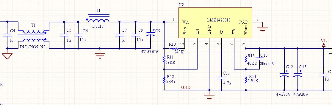
Other Parts Discussed in Thread: LMZ14203H, , LMZ14201

We use the LMZ1420xH series for many applications.

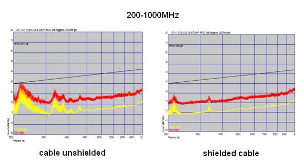
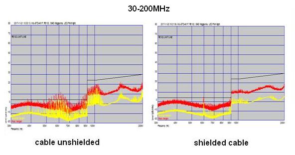
As already asked in the original thread, we experience EMI problems at 60-70MHz and 200MHz.

We tested different output capacitors combinations as recommended, nothing helps.

Initially we had a lot of problems also with conducted emissions, therefore the input stage is well filtered.

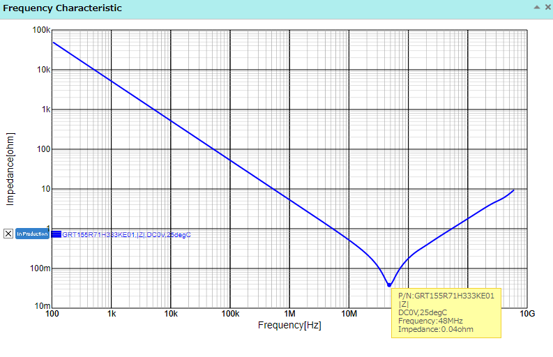
Just to mention that the LC filter recommended in the datasheet if far from responding as described.

Only with the addition of a large choke and ferrite beads we managed to keep it within the limits.

For this reason I tend to believe the emitted EMI is from the output stage.

But it seems that any attempt to add a filter only makes things worse.

Reading other threads I see that other users got the same results, e.g.

I will be glad to know if there is a solution, we use this series in very large quantities but the EMC compliance is a game stopper


  • Hi Emanuel,

    It sounds like you tried different values/combinations of high frequency input capacitors to reduce the noise but that wasn't enough to satisfy your design criteria? 

    Just to set the stage here, generally noise is created from the input path. The input supply, switching of HIGH and LOW MOSFETs and length of input lead inductance contribute to generating noise and then the package parasitic capacitance couples this noise onto the SW node of the circuit. This effectively results in the MHz-GHz range noise on the switching waveform and can be observed by using the probe to "sniff" around the part. 

    Usually placing high frequency capacitors close to the VIN and GND pin reduces the effective high di/dt loop that generates these noises as both emitted and radiated EMI. If that doesn't work, an input filter can be utilized to target the specific frequency. PCB layout techniques can be utilized to further design for EMI mitigating robustness through shielding, fencing, grounding techniques. Lastly a LDO can be cascaded at the output to generate a low noise output voltage rail. 

    For reference please take a look at some of our available app notes:

    Looking at the past EMI results what input voltage condition was this? Of course the larger the input voltage, the larger the SW node and larger the radiated EMI will be. I would design the filter for worse case application, high VIN at full load. 

    Regards,

    Jimmy 

  • Hi Jimmy,

    We experience the same emissions with all 3 modules, LMZ14201H, LMZ14201H and LMZ14203H in different products with different PCB.
    Most of our products work in 24V system automotive environment, all tested at 28V.

    The radiated peaks are at 70MHz and just above 200MHz.

     At this point we resolved the conducted emissions with the addition of ferrite beads (optimized for low frequency) on the input lines, a common mode choke (also optimized for low frequency) followed by a PI filter.

    The conducted emissions test is performed from 10KHz up to 10MHz, so the filtering described somehow works.

    We use a frequency of approx. 280KHz to keep the peak in the range of the test curve where the limit is in a down slope, from 10KHz to 500KHz.

    In the 500KHz to 10MHz we still see harmonies of the clock but they are below the limit.

    The PI filter has 2 capacitors at the input, 1u and 10u ceramic, a 3.3uH inductor and 3 capacitors at the output, 1u, 10u ceramic and 35u aluminum.

    At the LMZ output we use 2x47u tantalum and 1u ceramic. 

    The PI filter, according to the LMZ data sheets which recommend an LC filter with the same values is intended to reduce conducted emissions.

    But in practice, when we used it initially it was far from providing the plots as shown in the data sheet and we had to add the choke.

    The weird part is that the 70MHz peak is very clear, the entire plot is flat an quiet, then the peak that starts at 60MHz, top at 70MHz ending at 80MHz.

  • Hi Emanuel,

    Just to re-clarify in summary, you are using the recommended 3.3uH/1uH LC line filter for conducted readings. However you are not passing emissions because peaks at 70MHz and some above 200MHz are hitting the limit lines even after using the input filter and an additional common mode choke. Your application calls for 28Vin/11Vout @ 600mA which you showed radiated EMI results in the referenced thread (original question). 

    1. Do all three products on different PCB experience the same radiated peak around 70MHz and above 200MHz?
    2. Have you tried taking an un-grounded oscilloscope probe and "sniffing" around your board to find where the source of the 70MHz noise might be coming from? If not I'd recommend doing that to help pinpoint where this 70MHz might be coming from. 
    3. Have you tried removing the two alumimum electrolytic capacitors and place C9 as close as possible to the VIN pin, you might need to shave the soldermask to get closer to the VIN pin. Right now looking at the PCB layout from the referenced thread, the input filter makes takes on a L shape current loop which is rather far from the input pin.
      1. PCB recommendation 1: One thing I would say is that C9 is far from the input pin. At high frequency, the capacitor and input lead inductance can actually resonate which will couple noise onto the SW and effective increase EMI results. Because of this, it is always recommended to place the high frequency capacitor as close as possible to the input pin. If I were to redesign your PCB, I would put the two aluminum electrolytic capacitor before the inductor and shift the LC filter as close as possible to the VIN pin. This way the aluminum electrolytic capacitors with high ESR dampens the input lines (since the power supply could be far away from the VIN plane), then the LC filter is created to further attenuate switching supply noise.
      2. PCB recommendation 2: I'd also sprinkle several GND vias to help create an input/output fencing. Also having unbroken GND planes on top and bottom PCB with signal/power planes in the mid layers will result in the noise being effectively "sandwiched" in mid layer. This will help reduce radiated EMI as there is more ground plane to help decouple the noisy signal. 
    4. What is your input source coming from? Is it a noisy input supply or well control and regulated? 

    EMI mitigation design can be fairly extensive and takes several lab testing and iterations to get down correctly. The combination of the device's switching harmonics, PCB layout, local switching components noise coupling, and a plethora of factors could contribute to the EMI results. 

    Regards,

    Jimmy 

  • Hi Jimmy,

    Attached you can see the input filter we use, the output 47u capacitors are tantalum, C9 is aluminum, all others ceramic.

    The recommended LC filter was not sufficient, in order to pass the conducted emissions test, and we are talking about CE102 we made a filter that includes ferrite beads, choke and a PI filter with 3.3uH.

    The test is indeed made at 28VDC, in real life the source is a car battery system, however the test is made with a power supply.

    We use the LMZ in about 20 different products, but so far we tested only 3 of them, all have the same peaks at 70MHz and 200MHz.

    The output voltage is different in the various applications, the lowest is 11V and the highest 16V.

    The current is 350mA to 700mA in circuits where we use the LMZ14201H, 1.4A using LMZ14201H and we have one product with 2.5A using LMZ14203H.

    In most of the circuits the current consumption is variable, as the LMZ is used as a primary power supply. The current can be for example in the 1.4A circuit 50mA, 700Ma or 1400mA.

    The test is repeated for all the modes and we see the peaks in all of them, including during standby, where the current is only several miliamps and practically nothing else in the circuit works.

    Regarding the PCB layout, each product is different but the LMZ itself and the output capacitors are quite similar, the input filter however is routed in different ways due to space constraints, still no effect on the peaks.

    Most PCB we use are metal core, double sided. We don't need to add vias as the bottom side cannot be a ground plane, it is populated with other components.

    But as I write this reply I realize that the worse results from the 3 tests were from 2 FR boards. Both are double sided with most of the bottom side used as ground plane, in addition we make a large ground plane also on top. 

  • Hi Emanuel,

    I will have to take a deeper look into this to see if there is any history of the LMZ14201 device having any issue like this. 

    I want to point out that the EMI data seen in the datasheet showcases the combination of the device and PCB layout in addition to the LC filter to get those EMI results. Your EMI results will be different because of local noise sources, input/output conditions, and PCB layout. 

    Again, do you have you have local noisy sources that could couple / resonant with the circuit? Is there anything switching besides the LMZ14201 device on your PCB? 

    Are you okay with trying to add a LDO at the output to help attenuate the noise? The app note referred previously shows what to expect using a LDO as an output filter for noise.

    If not, it may make sense to redesign the circuit for EMI from the beginning. What is your attenuation needs? From the original post it looks like only the peak around 150MHz is the issue since it crosses your limit lines. Is the 70MHz peak also a concern even if it is below the limit line? What is the conducted EMI results of the board before the input filter (pi filter and ferrite bead) was added. A conducted EMI test of the board will help detail the system noise levels and give us an understanding of where to start. I'd expect to see a peak at the switching frequency and multiple peaks after for the sub harmonics. The input filter filter will then be design to attenuate the main switching frequency based on equation 12 since you mentioned you have different boards layout and different output voltages. Then we can start adding more high frequency capacitors to see if that helps knock down the higher frequency noise.

    Regards,

    Jimmy

  • Hi Jimmy,

    We are making automotive lamps for heavy duty applications. The lamps are in aluminum housing which is well grounded, but because light needs to go out there is always a part of the enclosure which allows EMI to go out.

    The LMZ is the only source of oscillations, it is used as a main power supply to stabilized the vehicle voltage to a lower voltage, from there each LED string is driven by linear drivers.

    In certain products we use PWM dimming, but this is not affecting the test results.

    As mentioned, the peaks show also in standby mode, where the LEDs are off, so even the linear drivers are not working.

    About the EMC test, it is MIL-STD-461. 

    The higher frequency peak is in most cases below the limit, this is true, at least when tested according to E and F versions of the standard.

    But we recently had a product required to pass version G, which calls for unshielded cable. I am attaching the results with and without shielded cable.

    It looks like some EMI goes out through the cables, but as radiated, not conducted.

    Regarding the use of an LDO, I think that even the lowest will have some 1.2V drop, at 0.7A or 1.4A this becomes a few watts which add really unwanted extra heat.

    An of course we are not sure the EMI's source is from the output stage.

    Do you think that we use too high values for the input capacitors? The lowest is 1uF, maybe changing to lower values?

  • Hi Emanuel,

    If we were to keep the circuit as is but try changing the input capacitor values this might work but require several test/retests. 

    I would suggest using high frequency capacitor values below 1uF to take advantage of the low impedance notch. 

    For example below is an image of a 33nF 0402 high frequency capacitor. Perhaps you can try using a 33nF to see if the 70MHz signal couples through this high frequency capacitor to ground. This should effectively reduce the EMI results since this capacitor provides a high frequency low impedance path for noise to flow through. 

    Again I want to reiterate that this high frequency capacitor(Chf) should be as close as possible to the VIN pin. Looking at your schematic (assuming this is how you laid out the PCB layout), the 33nF should take the place of C9. The reason why you want this as close as possible to the VIN pin is to reduce the interaction of the Chf and PCB parasitic inductance from the VIN copper pour which could reduce the effective noise attenuation of the Chf.

    For testing purposes, you may need to shave off the soldermask on the top layer to get the Chf as close as possible to the VIN pin and GND pour. Doing this will reduce the high di/dt loop and minimize any counteractive elements that can impact the Chf. 

    Regards,

    Jimmy 

  • Hi Emanuel,

    Do you have any update/feedback on your response?

    Regards,

    Jimmy