This thread has been locked.

If you have a related question, please click the "Ask a related question" button in the top right corner. The newly created question will be automatically linked to this question.

CSD17308Q3: MOS damage risk

Part Number: CSD17308Q3

Hi Sir,

customer use CSD17308 for super Cap application, there is currently a problem as follow:

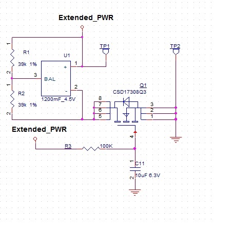
1. this is customer the schematic, R3 and C11 is soft start function but because there is already 2A of energy before reach the Vth voltage, will this factor cause the MOS to damage?

  if have any suggestion or idea,please kindly let us learn.

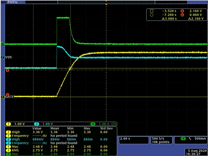
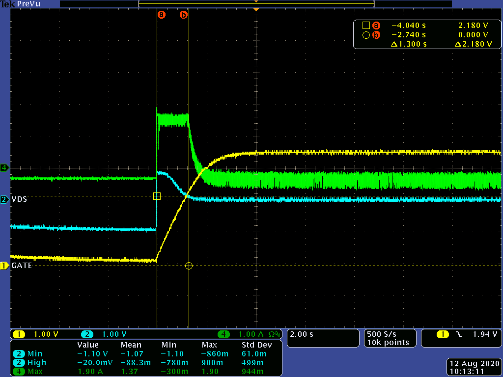
   please refer the as follow waveform.

Figure 1 (have C11_Cap)

ch1:Gate level

ch2:Vds

ch3:inrush cueernt

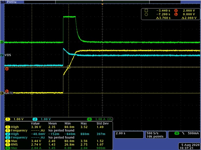
Figure 2 . (remove C11 cap)

ch1:Vgate level

ch2:Vds

ch3:inrush current

  • Hi Tommy,

    Thanks for promoting TI FETs at your customer. The first thing to consider is SOA (see Figure 10 in the datasheet) during the inrush event which lasts a little more than 1 second. In the first waveform, it appears VDS starts at a negative voltage and becomes +0.88V as the FET turns on and the drain current is 2A. These conditions are well within the SOA capabilities of the FET: 1V/100ms SOA current > 40A. This is a longer time period than we test but should be OK. The other thing to consider is the transient thermal impedance as shown in Figure 1 in the datasheet. For a 1 second, single pulse, this is essentially DC and the transient thermal impedance factor is 1. The calculated rise in TJ = 0.88V x 2A x 4.5degC/W = 7.92degC. This should also be OK but is dependent on the board layout & stackup and ambient conditions including Tamb and Tcase.

    Removing C11 speeds up turn on of the FET and the peak VDS is lower and it settles faster. This should reduce the power dissipation in the FET and temperature rise during the inrush transient.

    Is the customer having a problem in their application?

    Here are some links to useful information:

  • Hi Tommy,

    Following up to see if your issue is resolved or if you have additional questions or need more information. Please let me know.

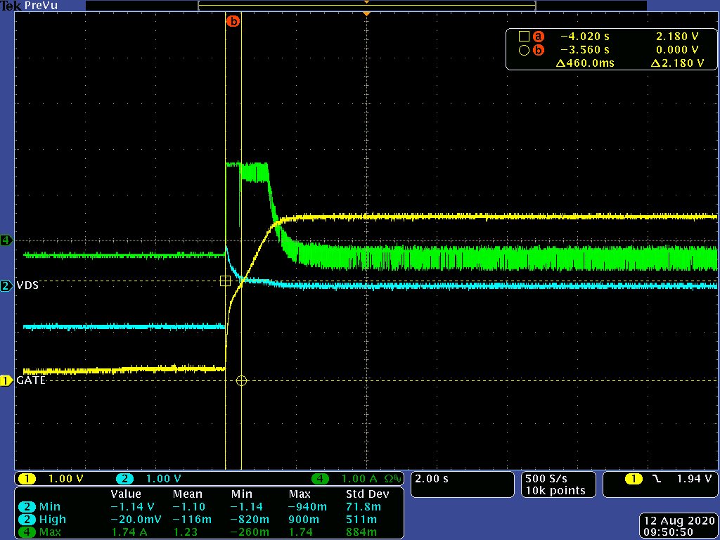
  • location R3 CHANGE TO 10K ohm as measurement again,any  best suggestions ?

    fig1 (R3:10K)

    ch1:Gate level

    ch2:Vds

    ch3:inrush cueernt

    fig2 (R3:100K)

    ch1:Gate level

    ch2:Vds

    ch3:inrush cueernt

  • Hi Vic,

    Thanks for the update. Can you please clarify if the customer is experiencing any problems or failures in their application? Is there concern that the current steps up to about 2A when the FET turns on? I don't see any problems with SOA or overstressing the FET with excessive power dissipation. Please let me know what the issue is.

  • Hi John

    Please see the under fig,my customer used power on/off several times,it happen the mosfet burning ,inrush about 2A as 1.3 second

  • HI Vic,

    Thanks for the update. I sent you a friend request and would like to continue this discussion on regular email. I will close this thread and wait for you to accept the friend request.

    In the meantime, I would like you to ask the customer to zoom in on the turn-on and turn-off of the FET. At 2s/div, it is very difficult to see any details on the waveforms. They can probably trigger the scope on VDS or ID. I'm looking to see if there is any excessive overshoot or undershoot of the drain current or drain-source voltage. Keep the same 3 waveforms. Just zoom in to a much smaller time scale so we can see the rising and falling edges of VDS and ID.

  • Hi Vic,

    Following up on the E2E inquiry. What is the failure rate of the CSD17308Q4 in your customer's application? Is this happening during development or is this in production? Can you please share the device markings on the top of the package.

    --------------------------------------------------------

    Replay

    Hi John

    This issue happen to one units,it's happen during product quality test.

  • Hi Vic,

    I am closing this thread and will contact you direclty via email.