Other Parts Discussed in Thread: LM5060
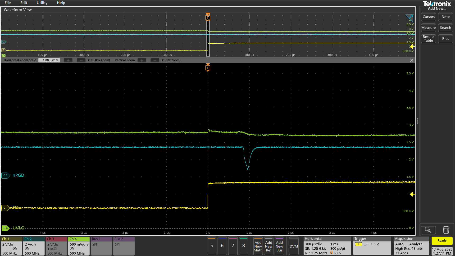
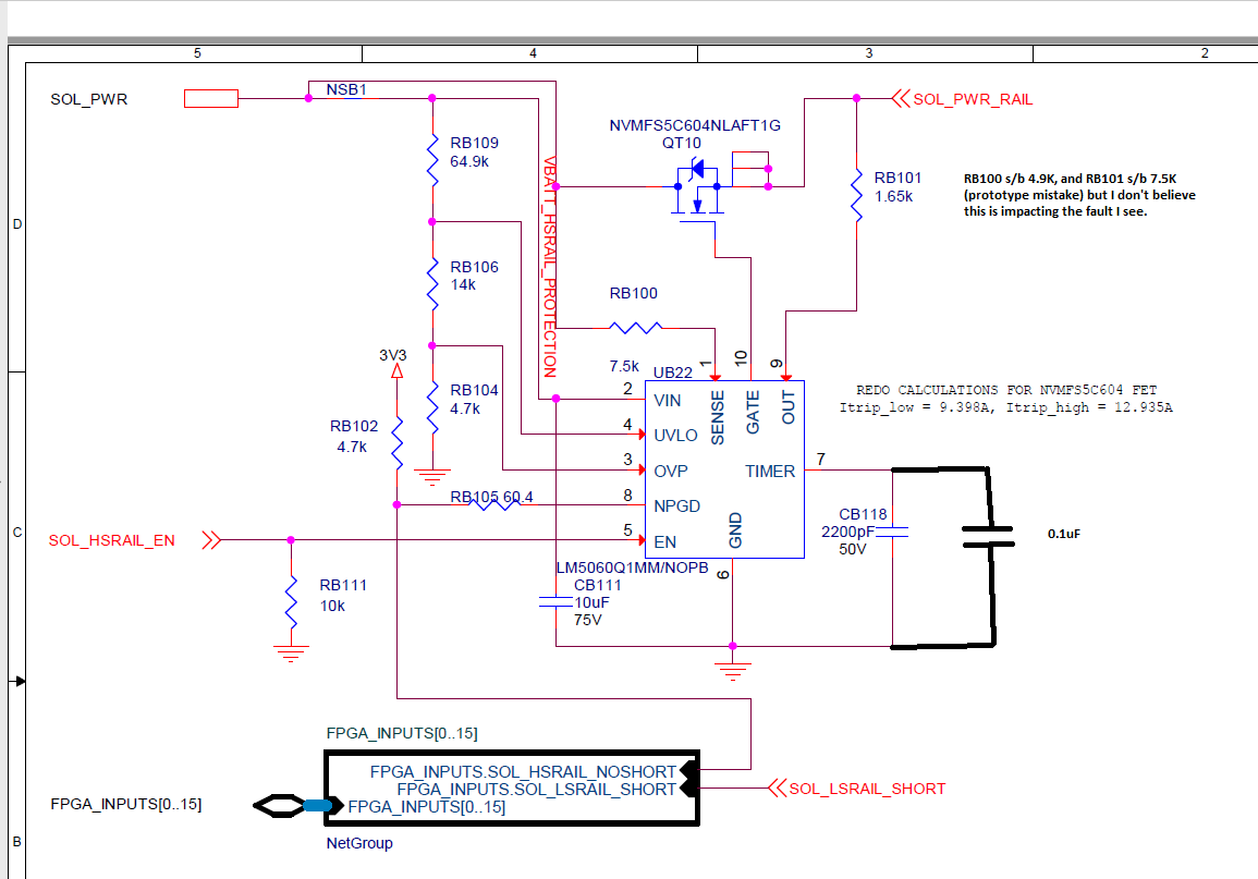
I am using an LM5060 gate driver to switch a common high side rail for 6 TPS1H100 high side drivers (the LM5060 is an emergency high side rail shutoff). The "LM5060-sch" file shows the relevant section of the schematic. An FPGA controls the EN input on the LM5060, and monitors the nPGD output. The FPGA has a state machine to control the LM5060; when the microcontroller want to turn on the rail, the FPGA starts a 3ms timer and asserts the EN input. If the timer expires before nPGD is asserted (goes low), a fault is flagged. Once nPGD goes low, the state machine transitions to the "ON" state and if nPGD negates during the state (goes high), a fault is flagged and EN is negated until the microcontroller shuts the rail off and tries to power up again.
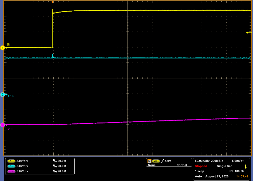
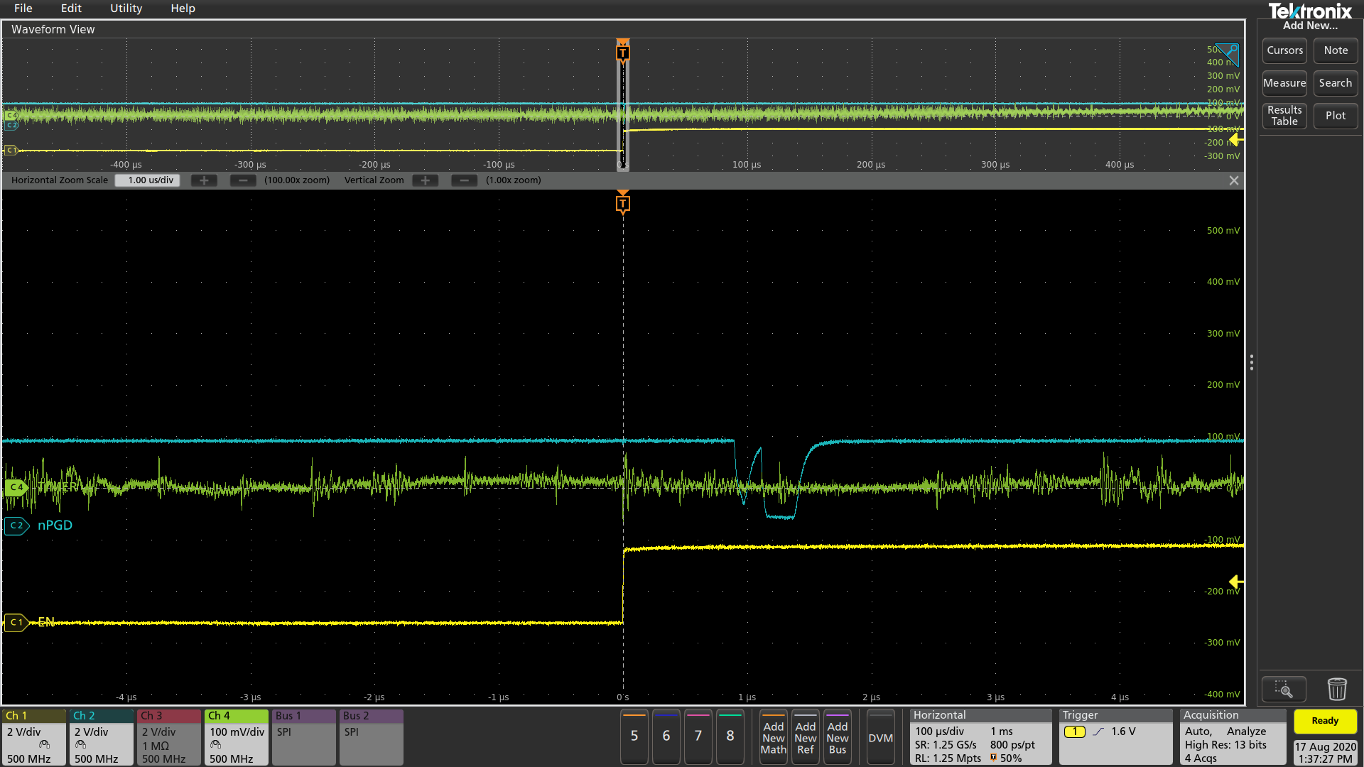
There is a brief glitch filter (~625ns) on the FPGA input from the nPGD pin to prevent external noise from tripping a fault. When I turn on the LM5060, there is a glitch on the nPGD output, which in certain cases exceeds the duration of my glitch filter, causing the FPGA to detect a fault (and turn off the LM5060). The attached "LM5060-GOOD" screen shot shows a successful startup, where the glitch is small (and is suppressed by the glitch filter). The "LM5060-BAD" screen shot shows a failure, where the glitch is of an extended duration, causing the FPGA to trap a fault and negate the EN command.
I have checked for ground bounce on the GND/VIN (CB111) decoupling (nothing), and on the +3.3V rail @ the RB102 pullup resistor. I could extend the glitch filter duration on the FPGA to get this to work, but before I do this, I'd like to know why this is happening.
The scope probe channels are connected to :
(1) EN pin (picked off at RB111, wire from LM5060 pin 5), ground @ TP1, which is a test point connected to the (digital) ground plane.
(2) nPGD pin (picked off at RB102, between pullup and series termination resistor, this is a 60-ohm transmission line)
(3) SENSE pin (picked off at LM5060 pin 1)
(4) OUT pin (picked off at RB101, wire from LM5060 pin 9)
(5) GATE pin (picked off at LM5060 pin 10)
(6) TIMER pin (picked off at CB118, wire from LM5060 pin 7)
(8) VIN pin, picked off at CB111+, probe ground at CB111-
The nPGD and EN traces run back to an FPGA. They eventually get near, and run adjacent to, two other traces which perform similar functions for the low side rail cutoff FET, however these signals are not being switched during this test. All of the FPGA signals were run through post-route SI switching simulations to ensure voltage compliance and no glitches (although no crosstalk simulations were performed). Right now there is no other activity on the board, other than power supply and internal microcontroller and FPGA clocking.
I'd like to know why I am seeing this glitch; I can see no power supply or SI reason for it, so I am leaning towards it being something internal to the LM5060. (I have already replaced the LM5060 once to see if the problem goes away.) According to the data sheet, the nPGD is an open-collector output driven by the VDS comparator, and should not be pulling the nPGD pin down until OUT voltage rises to the sense voltage. At this point in the turn on, SENSE is at 9V and OUT is still at around 0V. I've racked my brain and my only guess is that it has something to do with the 8/16uA current sources on the comparator inputs. Thanks, Glenn
#1: Schematic diagram of relevant circuit
#2: "Bad" turnon; nPGD has an extended glitch, and FPGA negates the EN signal, latching a fault.

#3: "Good" turn on; There is still a brief, unexplained glitch, but it is suppressed by the FPGA glitch filter.