This thread has been locked.

If you have a related question, please click the "Ask a related question" button in the top right corner. The newly created question will be automatically linked to this question.

TPS54A24: Noise on VIN and VOUT of power supply IC

Part Number: TPS54A24

I created a deign for the TPS54A24 on webench and put all the capacitors in the design, however my input and output are both still very noisy especially during loading. What are the possible solutions besides just gluing on more capacitors. 

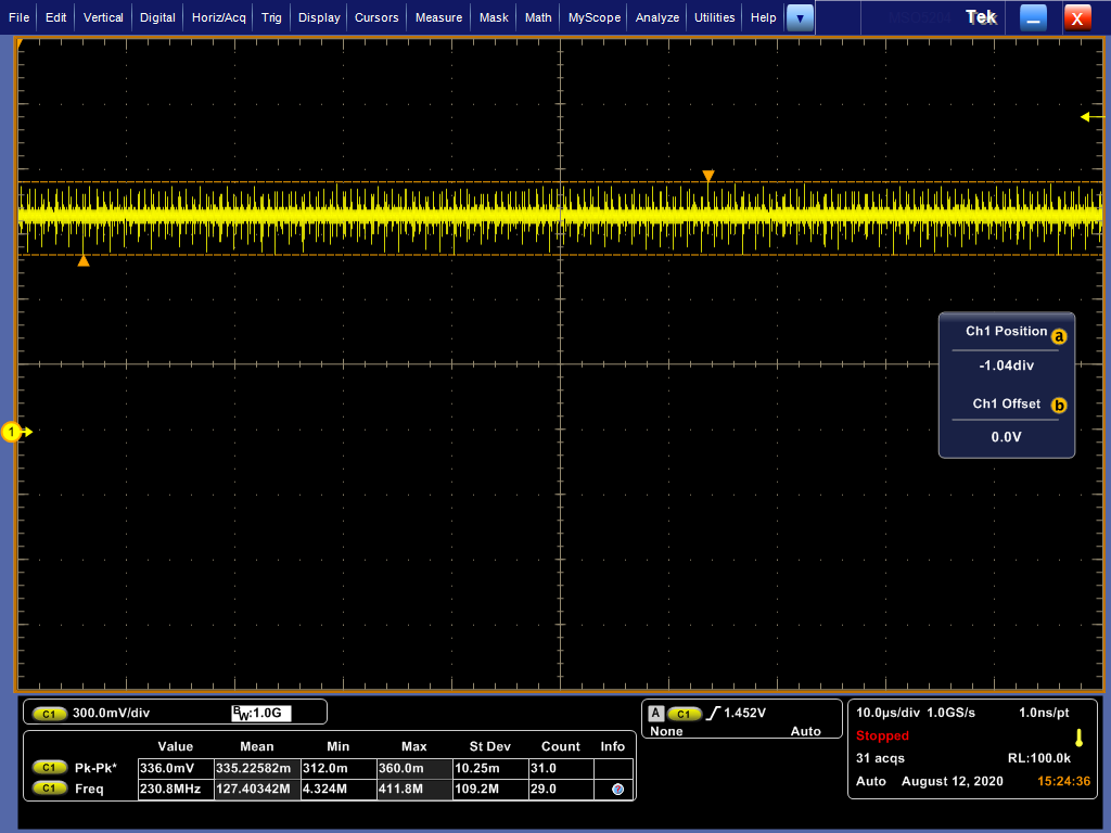
This first image is the 5V input rail during no load

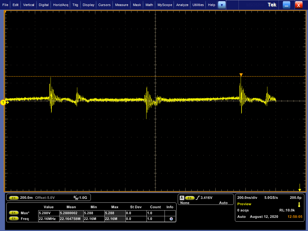
The second image is the 1v output rail in no load

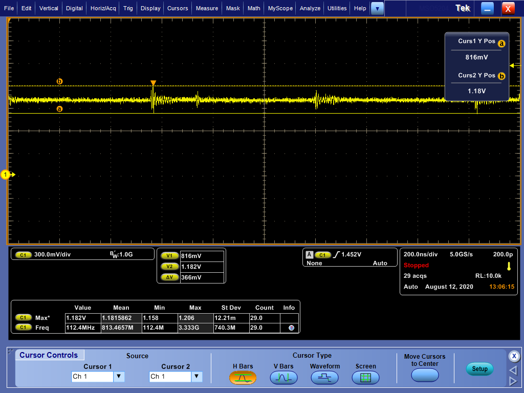
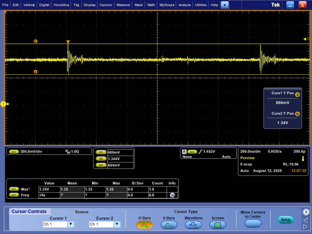
The third image is the 1v rail during a 0.6A load

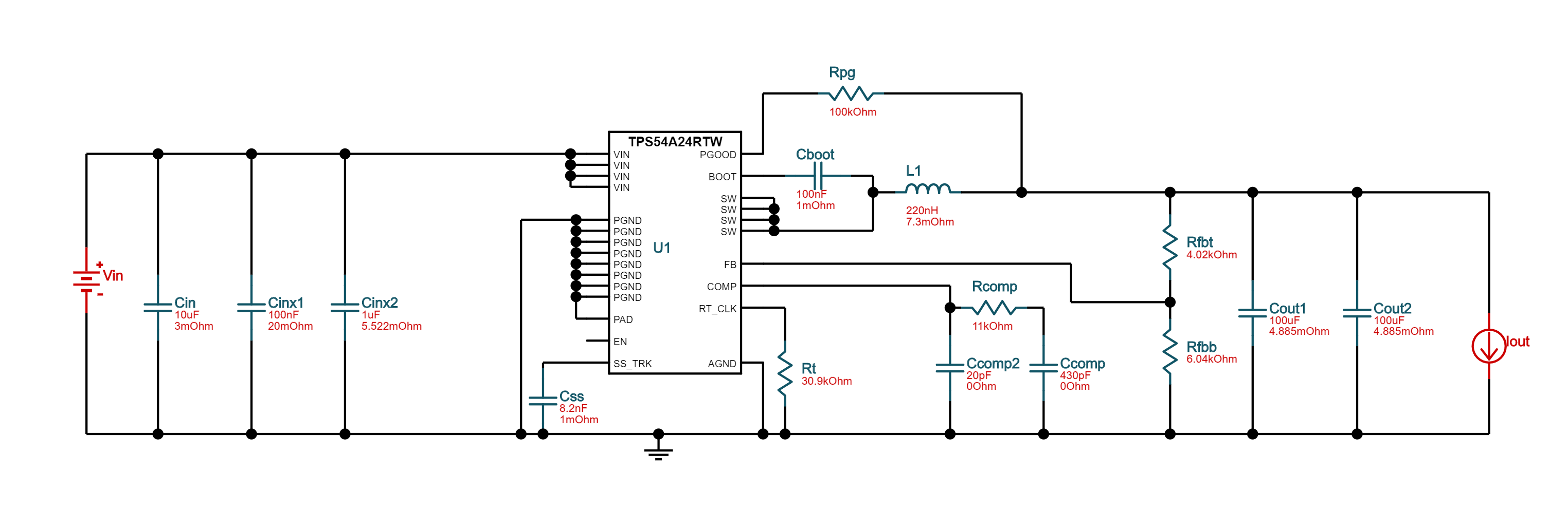
This is the webench schematic I used.

  • Hi Imraan,

    It is normal to see noise like this on the input and output of a buck converter. The high frequency noise comes from the rising edge and falling edge of SW node. There are things which can be done to reduce this noise such as adding a boot resistor or snubber, adding input or output caps for high frequency bypass or adding some inductive filtering.

    First I'd like to check, is this causing an issue in your application? Do you have a specific design target you need to meet?

    Thanks,
    Anthony

  • One of the issues is that we have another buck converter IC generating 5 other voltages, and when all voltages are enabled the noise in the 5Vin and all the output voltages gets much worse, with voltage swings of more than 330 mV. I have attached an image of what the 1v output looks like with all voltages enabled. I wasnt able to get a specific design target but this voltage is going to be used to power an FPGA and our engineer for that said these voltages are looking too noisy.

  • One of the issues is that we have another buck converter IC generating 5 other voltages, and when all voltages are enabled the noise in the 5Vin and all the output voltages gets much worse, with voltage swings of more than 330 mV. I have attached an image of what the 1v output looks like with all voltages enabled. I wasnt able to get a specific design target but this voltage is going to be used to power an FPGA and our engineer for that said these voltages are looking too noisy.

  • It seems part of the issue is noise from other converters as well? This could be related to noise picked up in the measurement.

    When measuring the output ripple with full bandwidth the measurement technique is very important and make sure you actually need to measure this with full bandwidth. This is why I'm trying to confirm if this is really a problem or just a measurement artifact. Thee high frequency component of the output ripple may not matter for the FPGA (and many other applications) so we typically measure with 20 MHz bandwidth limited. Depending on where this is being measured, the parasitic impedance of the PCB traces may even filter out the high frequency component before it gets to the FPGA.

    For measuring the output ripple it's important to minimize the loop area to avoid picking up noise. This can be done by doing a "pigtail" type measurement, using a differential probe or soldering a coax cable directly across the output caps. It is also probably best to prove the ripple as close as possible to the load. The tech article linked below does a good job discussing this if you'd like some more detail.

    https://e2e.ti.com/blogs_/b/powerhouse/archive/2016/07/27/how-you-measure-your-ripple-can-make-you-or-break-you

    If this noise really needs to get reduced, it will likely require some changes to the TPS54A24 and maybe some of the other regulators as based on my current understanding it seems like some of the noise is coming from other regulators. For reducing noise of the TPS54A24, the article linked below might also be useful.

    https://www.ti.com/lit/an/slyt740/slyt740.pdf