Hi Team,
Would you advise below 3 questions about heat radiation design?
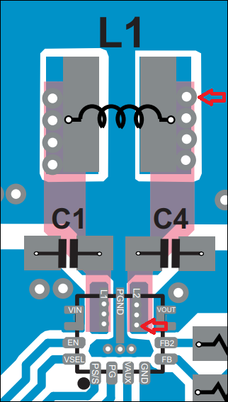
Regarding TPS63070 datasheet(Section 11.2 Layout Example) or
TPS630702EVM(Section 3.1 TPS630702EVM Layout).
1.I think that the measurement of the junction temperature is based on the standard test specified by JEDEC.
Is the layout proposed in the data sheet assuming a copper foil thickness of 70um?
2.What is the via size under the choke coil L1, L1 (9 Pin) and L2 (11 Pin) terminals of TPS63070 in the
layout example? Also, is the via below the L1/L2 terminals filled with holes?
3.What are the copper foil thickness (12um/18um/35um/70um) and the number of layers
(2 layers/4 layers) of the evaluation board? Also, is there any information such as the
recommended copper foil thickness or the copper foil thickness assumed in design?
Thanks
Best regards,
Shidara