This thread has been locked.

If you have a related question, please click the "Ask a related question" button in the top right corner. The newly created question will be automatically linked to this question.

LM25085: LM25085 Current limited too low

Part Number: LM25085

Hello,

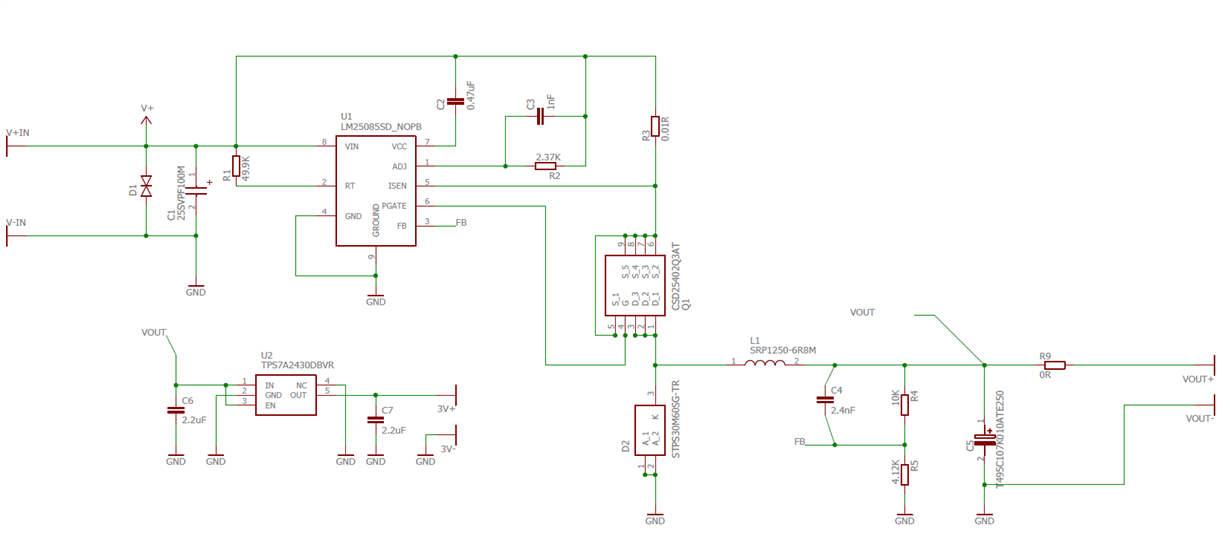
I used WEBENCH to design a regulator (VinMin = 4.5V VinMax = 16.0V Vout = 4.3V Iout = 5.5A), the main regulator is a LM25085 ( I use also a second LDO to generate a 2.5V for other purpose) , circuit is attached and also the WEBENCH report.

I have just get the PCB and the output is correct when there is no load (Vout = 4.3V).

When a load is connected (1 Ohm resistor) the current seems to be limited to 0.01A at Vin = 7V, and it drop to 0.002A at Vin = 11V.

I checked the components values and they seems OK. I have no idea how to debug the problem, any mistake on the circuit ? Any advice ?

Best regards,

RiccardoWBDesign22.pdf

  • Hello Riccardo,

    It sounds like your power supply may be hitting current limit. What is the current limit of your supply set to?

    Regards,

    Harrison Overturf

  • Hello,

    my power supply doesn't hit the current limit.

    To be sure I have made a test with 2 Ohm load, and my power supply have 3.1A limit, the behaviour hasn't changed.

    Regards,

    Riccardo

  • Hi Riccardo,

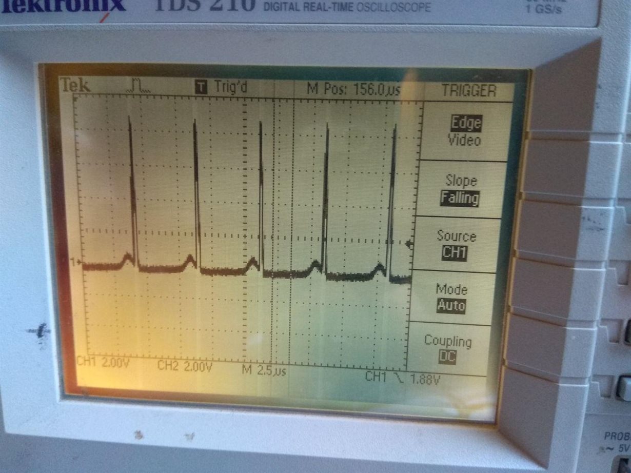
    Can you please send the following waveforms:

    Vin

    Vout

    Vsw (voltage across the D2 diode)

    VFB (take this measurement on its own with no other probes attached to the circuit)

    The above waveforms will help to confirm whether the device is unstable because of not enough ripple injection, see note below.

    After looking over your schematic I realized the following:

    Cff should be increased to 2700pF, and the ESR of the output capacitor should be increased to between 389mOhm to 655mOhm in order to ensure enough in- phase ripple is injected into the FB pin. These values were obtained from the device quick start calculator which is located in the product folder for the device.

    Regards,

    Harrison Overturf

  • Hello,

    thank you for the replay.

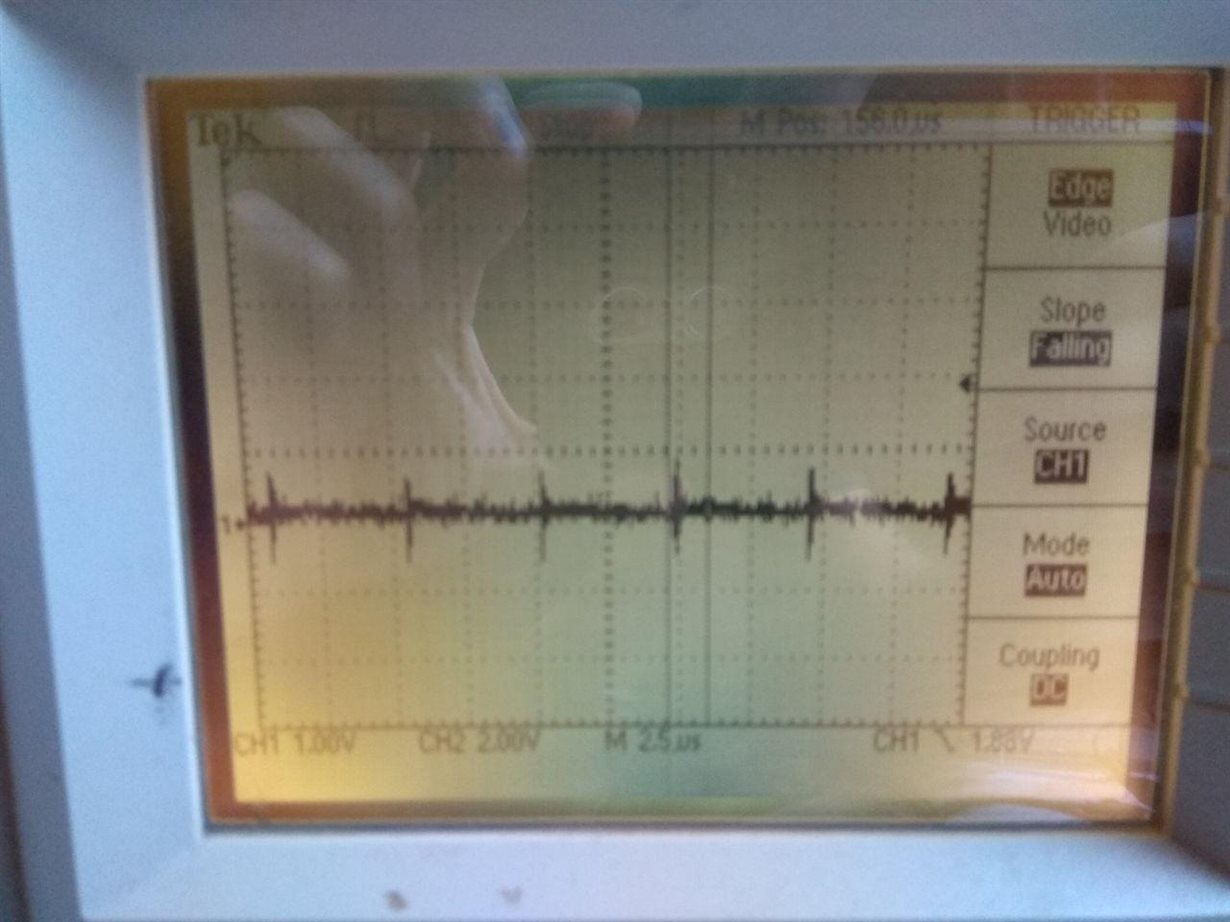
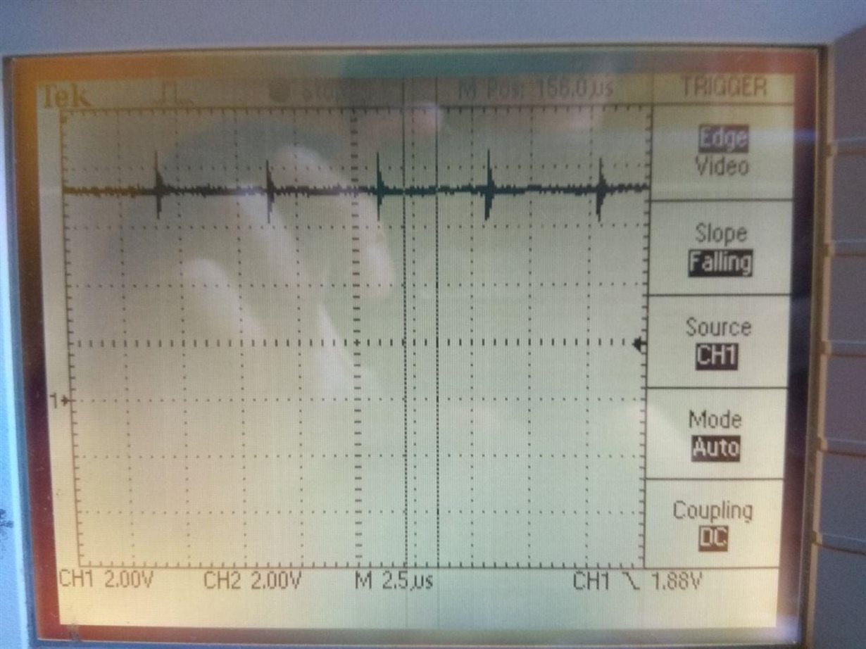
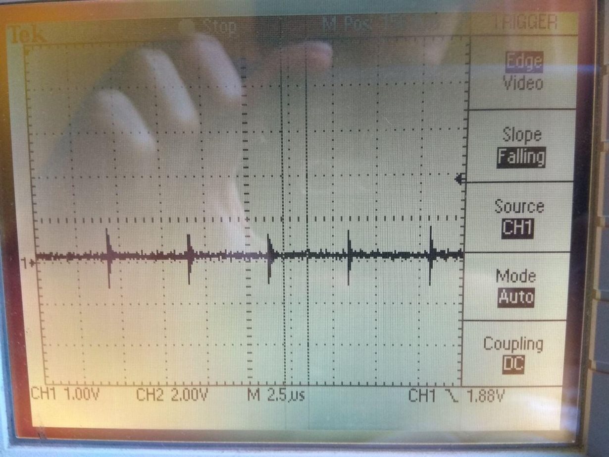
    Attached the waveforms, with load (2 Ohm) and without load. On the picture title the description.

    What do you suggest ?

    Regards

    Riccardo

  • Hi Riccardo,

    Thank you for the screen captures, can you please send me your board layout?

    Regards,

    Harrison Overturf

  • Hello,

    I have attached a .rar file with the gerber files.

    I have also attached 2 screenshot with the top and bottom layer, in case you have problem to open the gerbers.

    Best regards,
    Riccardo

    VREG_FLASH_V0.rar

  • Hi Riccardo,

    Thanks again for sending the scope shots and the layout.

    At this point I suggest the following:

    Cff should be increased to 2700pF, and the ESR of the output capacitor should be increased to between 389mOhm to 655mOhm in order to ensure enough in- phase ripple is injected into the FB pin. These values were obtained from the device quick start calculator which is located in the product folder for the device. I would double check your design using this calculator as the values it comes up with can be better than Webench.

    The following app. note is very helpful for understanding ripple injection when it comes to COT controllers.

    https://www.ti.com/lit/an/snva166a/snva166a.pdf?ts=1598558394905 

    Regards,

    Harrison Overturf

  • Hello,

    thank you for the response.

    I have to order the new components to make the test, meanwhile can I try to use the following values  ? :

    1) Cff = 3nF

    2) As for the output capacitor I have a 100uF 250mOhm capacitor on the board now, can I place two capacitor in series to have enough ESR ?

    Best regards,
    Riccardo

  • Riccardo,

    Yes Cff=3nF should be fine the calculator tool shows the minimum value being 2700pF, and placing the two capacitors in series should work as well.

    Regards,

    Harrison Overturf

  • Hello,

    I tried to place the two capacitor in series (to have 500mOhm of ESR), and to increase Cff to 2.7nF and then to 3.3nF, but the behaviour of the circuit didn't change (the waveforms are always the same).

    I don't know how I can fix the circuit, any advice?

    Regards,
    Riccardo

  • Hi Riccardo,

    Is there any load connected to the LDO while you are running these tests? I'm wondering if this is sinking all the current from your output capacitor which is causing your output voltage to drop. If your LDO is loaded, try removing the load and testing the circuit again. Can you please attempt the following test to ensure that your current limit is set to the correct value:

    1. Remove any load connected to either LDO or main output voltage terminal
    2. Measure output voltage and switch node voltage, you should see pulses similar to the ones you saw in the previous SW node loaded case, so zoom out the time scale to measure those pulses, record the output voltage.
    3. Place a 1kOhm load resistor across the load, repeat #2
    4. Repeat #3 for 500Ohm, 100Ohm, 50Ohm, 20Ohm, 10Ohm, 5Ohm...
    1. The resistor values aren't super critical, we are just trying to see ball park area of where the part stops regulating

    I'm hoping that the above test will show us where the device is entering into current limit, then from there we can work towards changing component values, if need be, to keep the part regulating properly.

    Regards,

    Harrison Overturf

  • Hello,

    I did some measurement, please see the attached report.

    It seems to me that between 47Ohm and 22Ohm the regulator start to reduce the Output.

    Report.docx

    Best regards

    Riccardo

  • Hello Riccardo,

    Thank you for the screenshots of your measurements. I was able to replicate your behavior via simulation (using your components values of course) for both the 100Ohm and 47Ohm cases, however at 22Ohms we run into problems. I believe the error is has more to do with board layout at this point more than anything else.

    In order to improve your layout I have a few suggestions:

    • Do not route the PGATE signal trace underneath your RSENSE resistor because this will cause your gate signal to become corrupted with noise from the power path at higher currents. In general you want to keep these types of control signals away from your power signals when you layout your board.
    • R2 and C3 should be placed as close as possible to pin 1 of the IC and should not be connected with a via as they are currently.

    Please refer to section 10 in the datasheet for the proper layout guidelines and for a good example of proper layout. Let me know if these changes result in improved performance.

    Regards,

    Harrison Overturf

  • Hello,

    thank you for the advice, I'll try to fix the layout.

    Regards

    Riccardo

  • Hi Riccardo,

    I'm going to close out this thread. If you are still experiencing issues after the layout changes, feel free to open this thread back up again.

    Regards,

    Harrison Overturf