This thread has been locked.

If you have a related question, please click the "Ask a related question" button in the top right corner. The newly created question will be automatically linked to this question.

TPS40303: Output couldn't restored if VDD(VIN) drop and restored

Part Number: TPS40303

Hi Team,

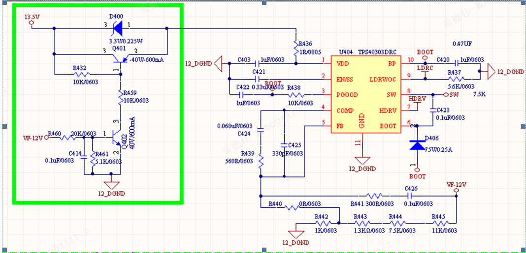
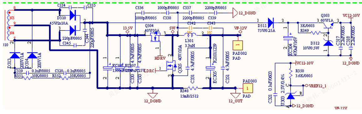
  My customer reported an issue that while the VDD drop and restored, the TPS40303 couldn’t provide normal output voltage.

The VDD provided by previous power module output which has the over current protection, if the load detected over setting which is less that TPS40303 OCP value, the VDD would pulled to less than 3V, and the PGOOD is pull to low. After the load removed, the VIN would be back to normal, but the output of TPS40303 couldn’t be restored.

 Support Needs:  

  • While the input restored, and output load is empty and couldn’t trigger OCP, From previous test waveform,

    why the PGOOD signal could be restored?  

  • How to fix this issue?

The detailed description/schematic&PCB Layout/test waveform could be found as attached file.

Expect for your kindly reply.

TPS40303 Could be restore issue.docx


Best Regards

Benjamin


  • Hi Benjamin

        A few questions

    1. Is the load applied to the TPS40303 or the power module that supplies the VDD?

    2. When you mention PGOOD is being restored, that means that TPS40303's Vout is 0V, but still PGOOD is showing ok?

    Regards,

    Gerold

  •  

    It looks like the converter is repeatedly triggering current limit.

    In figure 3, we can see repeated LDRV pulses, corresponding to the OCP limit timing on the EN/SS pin.  It's possible on one of the UVLO power cycles the current limit detection on LDRV got misread during power-up and the OC level is now wrong and low.  Since we don't see the output voltage coming up, it's also possible the boot-strap capacitor is not charged and can't turn-on the high-side FET, triggering high-side short circuit protection.

    The schematic provided in the file does not show the connections to the power FETs, and the layout does not show how the VDD pin is connected to the power-FETs either.

    How is R436 connected?  Is it between the drain of the high-side FET and the VDD pin?

    Where is VIN from the oscilloscope measured?  The Power FETs? VDD? R436?

    Is the power for VDD flowing through Q401?  I don't see any vias after Q401 or R436 that would connect it to the power-FETs.

    Can you measure VDD, BOOT, HDRV and LDRV during this over load and recovery as well as get the schematic that includes the power stage (FETs, Inductor and capacitor?

  • Hi  Gerold,


    1. Is the load applied to the TPS40303 or the power module that supplies the VDD?

    Benjamin:  the load is applied to TPS40303.     and TPS40303  VDD is powered by other power module which also has the OCP feature.

    2. When you mention PGOOD is being restored, that means that TPS40303's Vout is 0V, but still PGOOD is showing ok?

    Benjamin:  I've made a mistake,  the question is PGOOD is not being restored,  the question is why TPS40303 load is removed, and the input voltage restored to normal,  the PGOOD still not restored.  why this situation happened.

  •  Hi Benjamin

         Peter had a few questions. Can you please respond to those as well?

    Regards

    Gerold

  • Hi Peter,

      The TPS40303 related schematic shown as below 2 figures. For the test waveform,  the VIN is test at Drain of Q304.

      Another test is to decrease the R437 which decrease the OCP point, while system OCP happened and the VIN dropped, then remove the system OCP situation, the VIN restored, VOUT couldn't restore issue could be easily reproduced.  Seems the TPS40303 OCP always happened.

      Could you kindly give comments that why TPS40303 OCP situation couldn't cleared?


  • Hi Peter,

      Add test waveform for VDD/HDRV/LDRV/BOOT pin as below figure, from the figure, the input voltage has been restored to 10V and OCP situation has been eliminated.but the HDRV only with a small duty pulse and couldn't turn on the high side MOSFET.

      Could you kindly give comments on the reason the HDRV couldn't worked as normal,  also why the Soft-start couldn't work? Expect for your kindly reply, thanks.

    CH1:HDRV  CH2: VDD   CH3:Vboot->GND:   CH4: LDRV

  •  

    Can we get the VDD, BOOT, HDRV waveforms when the part is repeatedly tried to restart?

    Also, if you can get HDRV, SW and LDRV triggered on LDRV at about 1us per division and 1Vdivision on the SW, it would be good to see what SW is during the low-side FET ON-time so we can try and understand why the part is not restarting after 7 soft-start cycles.

  • It looks like you sent me what I was asking for while I was asking for it, please give me a minute to review the waveforms you sent.

  •  

    The reason the HDRV pulses are so short is because the part is trying to regulate to such a narrow on-time at the start of what appears to be an approximately 50ms soft-start time.  The HDRV pulse amplitude appears to be affected by the dV/dt of the switching node given high BOOT is rising.  It is likely that the Drain-Gate capacitance of the high-side FET is pushing back on the HDRV gate and preventing it from rising up.  I am surprised how fast the switch-node appears to be rising given the added capacitance on the switching node.

    The shut-down does appear to be OCP related with a LDRV pulse followed by no HDRV pulse.  At the same time, it looks like the ringing on the switch-node when the inductor current drops below zero is triggering the low-side OCP.

    1) Do we have the partnumber for the power-FETs? (Q304 and Q305)?

    2) Can we try reducing C421 to speed up the soft-start time?  It looks like it is currently 330nF, can we try reducing that to 33nF?

    3) Can we try removing C338 and replacing C337 with a 1-ohm resistor?

  • Hi Peter,

      The MOSFET part numbers are VISHAY(Si4840BDY-T1-GE3)、ONSEMI(FDS8447)、INFINEON(IRF7470PbF).

      Also tried to remove C336/C338/C337/C339,  the issue still exist but with low ratio to reproduce the issue.   and for decrease the capacitor of SS is in testing now.

    Best Regards

    Benjamin

  • Thank you Benjamin,

    Let me know how that goes.

    It would seem like the resonant ringing on the switching node after the inductor current drops to zero is triggering the low-side OCP when it tries to restart.  Let me know how reducing the soft-start capacitor goes.