This thread has been locked.

If you have a related question, please click the "Ask a related question" button in the top right corner. The newly created question will be automatically linked to this question.

TPS63001: TPS63001

Part Number: TPS63001

Hi everybody!

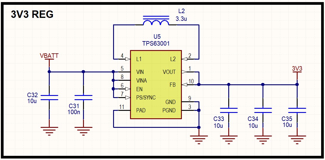
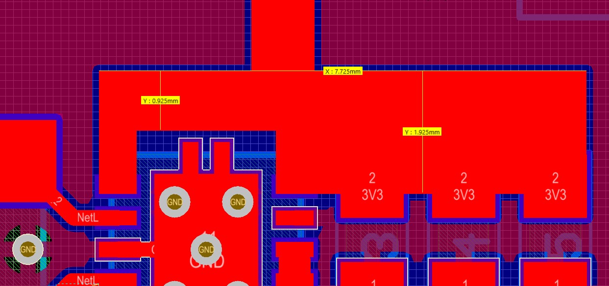
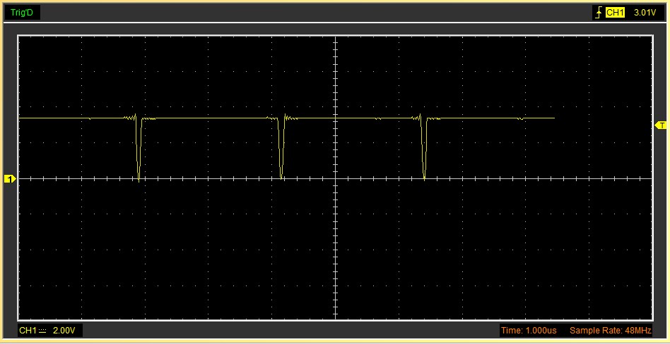
I designed a 3.3V regulator using the TPS63001 and components sugested by WEBENCH. The power is supplied by an one cell Li-ion Battery. But it doesn't work. The battery voltage is 3.4V. The waveform at pin 4 (L1) shows around 450kHz signal. And worse, without load (when my circuit  is in sleep mode), the regulator, only it, drains 3.8mA from battery. At work, the load drains around 25mA. Attached are the schematic, the circuit layout and the waveform at pin L1. The part numbers of C32~C35 is 0603ZD106KAT2A from AVX and the inductor is VLS4012HBX-3R3M from TDK. 

  • Hi Dalton:

    May I know the details that you mean "doesn't work"? Is it can't regulate 3.3V or even no any output voltage?

    Please share the Vin, Vout, L1,L2 waveform with me. Thank you! 

    Besides, the layout is not good, please refer the layout guidance in datasheet. "As for all switching power supplies, the layout is an important step in the design, especially at high peak currents and high switching frequencies. If the layout is not carefully done, the regulator could show stability problems as well as EMI problems. Therefore, use wide and short traces for the main current path and for the power ground tracks. The input capacitor, output capacitor, and the inductor should be placed as close as possible to the IC."

  • Hi Minqiu!

    Thank You very much for quick repply!!! I mean that switch frequency is out of range showed in datasheet and that IC is draining 3.8mA without load.

    I get 3.3V at output.

    The waveforms that you please are attached. (waveform on L1 I was attached in my post).

    Please, tell me what is wrong in my layout. The inductor is 0.7mm from IC terminals. The output trace has 1mm wide!

    Regards.

    Dalton

  • Hi Dalton:

    According the layout you shared first time, the C32, C31 is far away from IC. You could put then as close as possible to the IC. And for the output side, it's also recommend to modify the layout to reduce the parasitic parameters.(Better connection with Ground)  You can take datasheet 

    For power save mode, To enable power-save mode, PS/SYNC must be set low. Other wise the converter will keep switching, even there is no load. And the efficiency is low. 

    For the frequency, as the Vin is close to Vout, it will operation between Buck and Boost mode, like Fig11 in datasheet. So the frequency should be double what you observed 

  • Ok!

    I'll try.

    Thank you!