This thread has been locked.

If you have a related question, please click the "Ask a related question" button in the top right corner. The newly created question will be automatically linked to this question.

LM5113: Half bridge using LM5113 isn't work properly.

Part Number: LM5113

Good morning. 

I'm evaluating the EPC9055 GaN module which using LM5113 as a gate driver for GaN MOSFETs.  

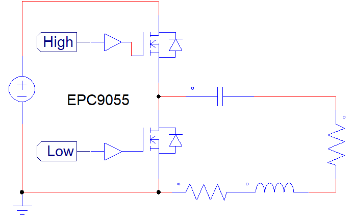
First of all, my final goal is to operate the circuit below. 

But it won't work. Power didn't flow to the output. 

After I check the waveform, the EPC9055 output is not working properly. it isn't a square wave. 

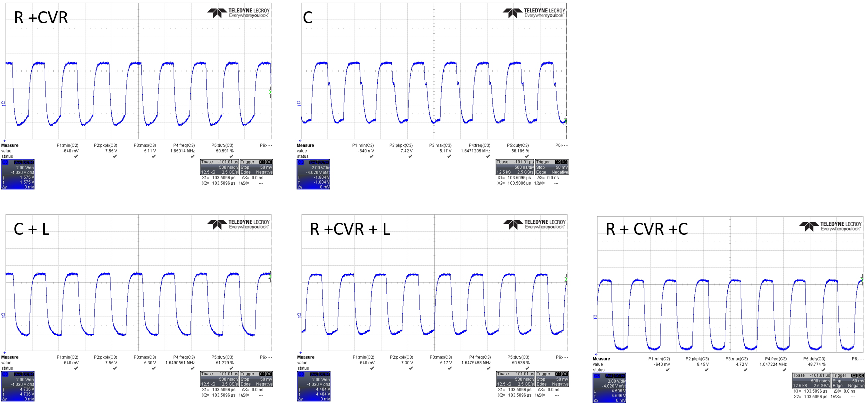
So I detached the full-wave rectifier part, re-checked the output of the EPC9055 like the circuit below. 

Note that the Capacitor and Inductor in the output side circuit of EPC9055 works in the Resonance point.  

The Center-bottom resistor is the PCB path resistor and the right side of the resistor is the load resistor which is several ohm(<10ohm). 

With this condition, also didn't work properly. 

After I check the gate driver in EPC9055, they use LM5113 as a gate driver and they are bootstrap type, Half-bridge driver. 

To drive bootstrap type driver, the drain-source of the bottom switch should be connected with the load as the figure below. 

I tried to add 10ohm as the load resistor, run the EPC5099 at the 1 Mhz PWM frequency. 

it worked properly I guessed as the figure below. 

So the question is, 

1. If it is the path to charge the bootstrap capacitor is like the figure below,

What is the difference between using the only resistor as the load resistor and the RLC circuit as the load at the resonance frequency?

because the typical LLC converter uses the half-bridge as the input.  

2. If it isn't working at my circuit, what should I add a component to charge the bootstrap capacitor?

Thank you for your help. 

  • Hi, Kyoungtak, Please review this tech note on bootstrap. Let us know if you have further questions after reviewing it. https://www.ti.com/lit/an/slua887/slua887.pdf?ts=1599496755145&ref_url=https%253A%252F%252Fwww.google.com%252F
  • Thank you for offering a useful document. 

    After I reviewed the document, the charging current of the bootstrap capacitor go through the bottom MOSFET while on state NOT load resistance. 

    Then I'm confused about malfunction without load resistance. 

    The further question is. 

    1. Can this LM5113 drive the half-bridge without load resistance? 

    In my experiment, when I attached 10 ohm to 50 ohm as a load resistance, the output of half-bridge(Drain-source of bottom MOSFET) 

    shows the square wave properly. but the no-load condition, it seems like bottom MOSFET wasn't turned on and off.

    Thank you for your help. 

  • Hi Kyoungtak,

    Thanks for reaching out!


    Could you please provide a full schematic including the driver and the circuitry around it?

    This is interesting as when the load is purely resistive, the bootstrap capacitor always has a resistive path to GND regardless of the state of the low-side FET… With the RLC load, the load charges and discharges at the switching node.

    Thanks,

    Aaron Grgurich

  • Thank you for your response. 

    Here is the schematic of EPC9055

    Following is the result of attaching RLC to the SW node and gnd of EPC9055

    Note that 12.8ohm has parasitic inductance around 4uH,

    the resonance frequency which is the same as the PWM frequency of EPC9055 is around 1.63MHz. 

    0.1ohm resistor is a Current Viewing Resistor(CVR) for current measurement. 

    and the next figure is the condition that the capacitor is connected to the ground.

    Following is the result waveform of different load types respectively. 

    My question is 

    what is the effect of the load to the LM5113 Half-bridge driver(Bootstrap type) or GaN MOSFET. 

    I was wondering if there is the reason why this circuit works wrong and the path to the solution. 

    Thank you for your help. 

    Have a nice day. 

  • Kyoungtak,

    There are a couple of things you may want to look into. Confirm that the V_DD voltage supplied to the LM5113 is within the 4.5V to 5.5V range (along with other recommended voltages).

    Next, the V_DD bypass capacitor is too small relative to the bootstrap capacitor for the driver (please refer to page 10 of the LM5113 datasheet). A good rule of thumb is to make the bypass capacitor >=10 times larger than the bootstrap capacitor, because the bypass capacitor is responsible for helping supply the bootstrap capacitor along with other local power needs.

    Regarding the effect the load has on the driver, if the load does not allow the switch node (V_HS) to pull close enough to GND when the low-side FET is on, then C_boot will not be able to charge enough to drive the high-side gate. As a result, the C_boot voltage will be depleted below the V_HB_HS UVLO threshold.


    Thanks,

    Aaron Grgurich

  • I'm sorry that I reply to this late. 

    Cause my eval board is broken while I measure the point.

    I'm waiting for new one that I ordered. 

    I'll reply after I get the new one.

    Thank you for your help. 

  • Kyoungtak,

    No worries, we will be here when you are ready.

    Thanks!

    Aaron Grgurich