This thread has been locked.

If you have a related question, please click the "Ask a related question" button in the top right corner. The newly created question will be automatically linked to this question.

UCD3138FW-PSFB: UCD3138-PSFB EVM no-load and dead-load problems

Part Number: UCD3138FW-PSFB

Hello

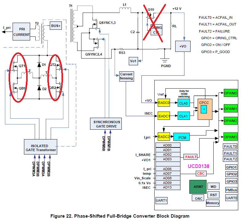
I recently tested UCD3138-PSFB EVM and found two problems:

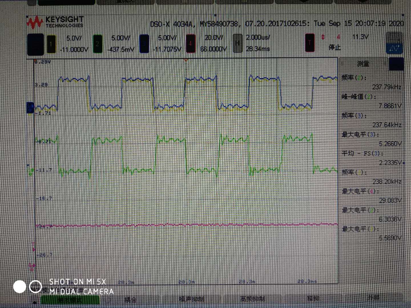
1. When the development board is unloaded and slightly loaded, the phase shift angle of the primary switch tube is very different. When there is no load, the phase shift angle is large. At light load and full load, the phase shift angle is small and the difference is not big.

why is it like this?

2. If the dead load on the development board is removed, the output voltage will drift up.

Why must add 20mA dead load?

  • Hi, Zoujiangyilang,

    At light load, SR is turned off. Power stage enters DCM mode, so the phase shift angle is large and sometimes DPWMs are on or off. The output ripple is bigger. There is offset on EAP2, can you measure what is the voltage  offset when power stage is disabled.

    Thanks,

    Sean

  • Hello,Sean.

    the previous problem has been solved. I now have another problem. The phenomenon is this:
    The circuit block diagram is similar to the development board, as shown below:

    1. The prototype can be started normally in the case of open-loop Schottky rectification;

    2. The prototype can be started normally in the case of open-loop synchronization;

    3. The prototype can be started normally in the case of closed-loop Schottky rectification;

    4. In the case of closed-loop synchronous rectification, the prototype can work normally if the load is 1A and 1A gradually loaded. After the output current to be greater than 5A, the synchronous rectification is turned on.

    5. But when the prototype is started directly from a 5A load, the Schottky diode connected in parallel with the secondary synchronous rectifier will be damaged. The startup transient waveform is as follows:

    In this starting process, when Vo reaches the set value of 28V, the synchronous rectification drive is turned on. The circuit was abnormal after working for 20ms. The 20ms drive waveform is divided into three states, as shown in the figure 1, 2 and 3.

    The first part of the waveform is as follows, the timing of the blue synchronous rectification drive wave and the yellow and green primary down tube drive waves are normal;


    The second part of the waveform is as follows. The timing of the blue synchronous rectification drive wave and the yellow and green primary down tube drive wave is abnormal;


    The third part of the waveform is as follows, the timing of the blue synchronous rectification drive wave and the yellow primary down tube drive wave are disordered;

    I imitated the development board to design the hardware and software. In terms of hardware, I made two changes:

    1. Eliminate the oring control circuit;
    2. Change the primary circuit of the main circuit from the leading type to the lagging type, that is, to move the position of the resonant inductor and the clamping diode to another bridge arm;

    In terms of software, no major changes have been made.


    I don't know why this happens?

  • Hello,

    In the system_defines.h, can you make the below change?

    change: #define PCM_BLANK   (30) 

    to: #define PCM_BLANK   (200) 

    Please let me know if it helps.

    Thanks,
    Sean

  • Thanks, let me have a try.

    Yesterday, I delayed the synchronous rectification signal by 1s and then turned it on.

    The prototype can be started with heavy load and closed loop.

    I suspect that it may cause the 3138 false protection due to the interference signal at the moment of activation.

    I don't know what you think?

  • Hello,Sean

    I tried to increase PCM_BLANK to 100ns and 150ns, the prototype can be started, the waveform is as follows:

    In the above figure, the blue is a secondary synchronous rectification driving PWM, and the red is the waveform of the output voltage Vo.

    The prototype can be started, but Vo still has about 100ms jitter.

    I don't know why this is? Is the blank not big enough? When the tube was blown up earlier, Vo was shaking.

    The blue waveform in the above figure is the primary peak current sampling waveform Ipri.

    Compared with your development board, the waveform jitter is severe, and the triangle of Ipri is not obvious, and the slope is low.

    I don’t know how I can improve this Ipri. Can I increase the slope compensation in the software to increase the slope of this Ipri?

    Thank you.

  • How much can this blanking value increase? Is there any bad effect on the circuit?

  • Isn't this external hardware slope compensation circuit added on the development board, but a DC level of about 100mV is added?

    Is the slope compensation compensated by software? How to modify the software to increase the slope compensation slope?