This thread has been locked.

If you have a related question, please click the "Ask a related question" button in the top right corner. The newly created question will be automatically linked to this question.

UCD3138064: OPEN/SHORT test on UC3138064 XTAL_IN and XTAL_OUT

Part Number: UCD3138064
Other Parts Discussed in Thread: UCD3138128A, UCD3138

Hi Expert,

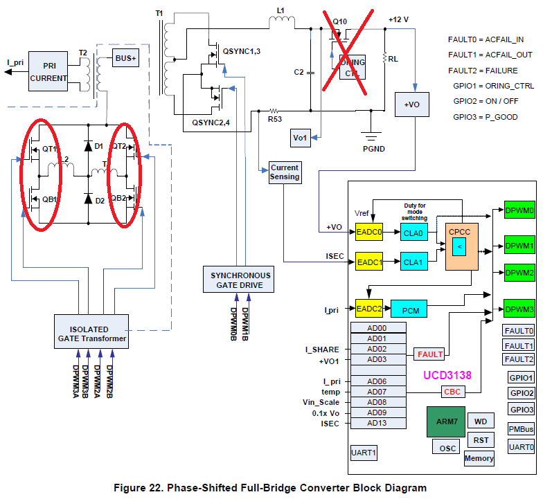
The engineer is conducting the open/short test on UC3138064 XTAL_IN and XTAL_OUT.

Pls advice the expected results for open/short the XTAL_IN and XTAL_OUT.

Thanks


Best regards,

Eric Lai


Field Application Engineer

Texas Instruments Taiwan Limited

O: +886-2-2175-2582

M: +886-909-262-582

E-Mail:Eric.Lai@ti.com     

  • Eric, I don't expect open and short to cause any problems, but I'm not sure.  I've put the question to the design team, but I don't know when I will get an answer.  I will give you a progress report tomorrow if I don't hear back sooner.  

    I'm assuming you mean one or more of the following shorts:

    1. short pins to each other

    2. short pins to ground

    3. Short pins to 3.3 volts

    I'm also assuming you really mean the UCD3138128A, since it is the only device with these pins.  

  • Eric, we think that it is not recommended to pull these pins up to 3.3 volts, as the are connected to the internal 1.8 volts.  They can be connected to the 1.8 volt pin.  It should be safe from a device damage point of view to pull them to ground or 1.8 volts.

    The design expert is working on the final stages of a design release, so detailed answers may not be quick.

    He did say that the system impact will be based on the configuration of the clock logic block in the CONFIG_INCL register.

    Obviously the clock will not operate properly if it isn't getting a correct input signal.  

    Note also that the only comment about these pins in the data sheet is as follows:

    If the XTAL_IN (Pin 61) and XTAL_OUT (Pin 62) are not used for external clock, tie them to 1.8 V (Pin BP18) through a 1-kΩ resistor respectively

    If the customer wants to be safe, this is what we recommend.  They are not general purpose I/O pins, they are dedicated crystal oscillator pins.  

  • Hello,Bower

    I encountered a problem while debugging a phase-shifted full-bridge power supply based on UCD3138.

    The phenomenon is this:

    The circuit block diagram is similar to the development board, as shown below:

    1. The prototype can be started normally in the case of open-loop Schottky rectification;

    2. The prototype can be started normally in the case of open-loop synchronization;

    3. The prototype can be started normally in the case of closed-loop Schottky rectification;

    4. In the case of closed-loop synchronous rectification, the prototype can work normally if the load is 1A and 1A gradually loaded. After the output current to be greater than 5A, the synchronous rectification is turned on.

    5. But when the prototype is started directly from a 5A load, the Schottky diode connected in parallel with the secondary synchronous rectifier will be damaged. The startup transient waveform is as follows:

    In this starting process, when Vo reaches the set value of 28V, the synchronous rectification drive is turned on. The circuit was abnormal after working for 20ms. The 20ms drive waveform is divided into three states, as shown in the figure 1, 2 and 3.

    The first part of the waveform is as follows, the timing of the blue synchronous rectification drive wave and the yellow and green primary down tube drive waves are normal;


    The second part of the waveform is as follows. The timing of the blue synchronous rectification drive wave and the yellow and green primary down tube drive wave is abnormal;


    The third part of the waveform is as follows, the timing of the blue synchronous rectification drive wave and the yellow primary down tube drive wave are disordered;

    I imitated the development board to design the hardware and software. In terms of hardware, I made two changes:

    1. Eliminate the oring control circuit;
    2. Change the primary circuit of the main circuit from the leading type to the lagging type, that is, to move the position of the resonant inductor and the clamping diode to another bridge arm;

    In terms of software, no major changes have been made.

    Recently, I delayed the synchronous rectification signal by 1s and then turned it on. The prototype can be started normally with heavy load.

    I suspect that some interference signal at the moment of starting triggered the UCD3138 error protection and caused the PWM timing disorder.

     what do you think?I don't know why this happens?

    Thanks.

  • Hello,Bower

    I tried to increase PCM_BLANK to 100ns and 150ns, the prototype can be started, the waveform is as follows:

    In the above figure, the blue is a secondary synchronous rectification driving PWM, and the red is the waveform of the output voltage Vo.

    The prototype can be started, but Vo still has about 100ms jitter.

    I don't know why this is? Is the blank not big enough? When the tube was blown up earlier, Vo was shaking.

    The blue waveform in the above figure is the primary peak current sampling waveform Ipri.

    Compared with your development board, the waveform jitter is severe, and the triangle of Ipri is not obvious, and the slope is low.

    I don’t know how I can improve this Ipri. Can I increase the slope compensation in the software to increase the slope of this Ipri?

    Thank you.

  • In the future, please start a new thread for a new question.  This is in the middle of an ongoing different thread, it makes it inconvenient for both the other thread and for future searches for this information.  

    Also if you start a new thread, all the experts will see it, and it will be possible to assign it to the best person.  

    I'm not the right person for this, so I will assign it to someone who is.  

  • OK,I know it.

    Thank you all the same.

    regards,

    ZJYL