This thread has been locked.

If you have a related question, please click the "Ask a related question" button in the top right corner. The newly created question will be automatically linked to this question.

UCC27211: Immediate failure with motor connected.

Part Number: UCC27211

Hi there,

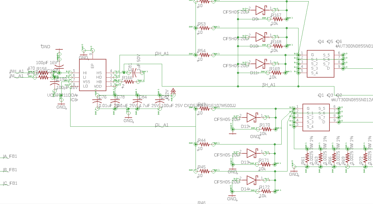
I have designed a 50V 5KW motor controller board with the UCC27211 where I am switching 3 mosfets in parallel. Each of the 3 UCC27211 is driving 3 x IAUT300N08S5N012 mosfets in parallel via independant 10 Ohm gate resistors. Please see the layout of the UCC27211 below. There is a lot if bulk capacitance in the system and I have a lot of decoupling capacitance at VDD Pin1.  The switching signals seems to be okay without the motor connected but as soon as the PWM is started with the motor connected the IC fails immediately with a burn mark right next to PIN1. What can I do to diagnose the problem?

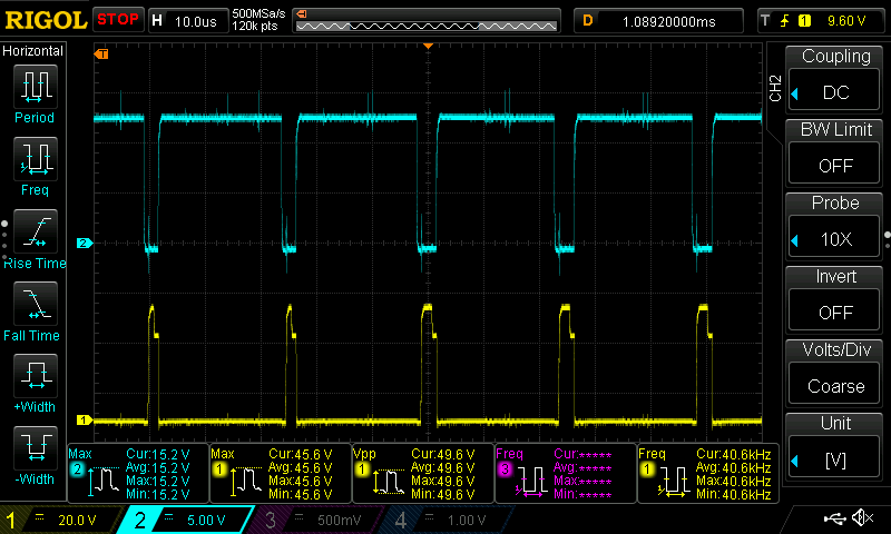
I have attached scopes of the inputs of the UCC27211 HI and LI pins, as well as the input at one of the mosfet Gate pins on the High side and Low side. The frequency is 40 Khz. I am using a 50V 1uF cap similar to the TI reference design: TIDUCB6, although they are targeting lower frequencies.

One thing to note: At the time of failure the battery voltage was quite low, I wonder if sudden shut-off could have anything to do with it?  

  •  Further Update, I measured between R166 and C81 to GND and I am seeing a huge spike. Any idea what is causing this? Is this capacitor not rated highly enough (It is 50V like the reference design)?   

  • Hello Steven,

    Thank you for the interest in the UCC27211. After reviewing the schematic and MOSFET datasheet I have some comments. The MOSFETs gate charge is fairly high at 178nC each which is 534nC total or ~0.5uF. I would review the data sheet design procedure or better yet refer to a newer driver datasheet that has more detail in the design process. The UCC27282 is a newer half bridge driver which can be used to reference the component value calculation for the UCC27211.

    I see on the schematic the HB to HS capacitance is 1uF which is not adequate to drive ~0.5uF gate charge. You will need a larger boot capacitor value more likely in the range of 3.3 to 4.7uF. When using a boot capacitance this high I would recommend having an external boot diode connected as close as possible to the IC VDD and HB pins. This placement is critical for the external diode to share the boot cap charging current. Use a fast recovery diode, Schottky diode if possible with an adequate reverse voltage rating and 1A average current rating. Use a small SMT package to allow placement close to the IC pins.

    If the boot cap is increased we also recommend a VDD capacitance that is 10x the boot capacitance close to the driver IC. I see on the schematic there is a large VDD capacitance, but on the layout I do not see that close to the IC pins. The boot capacitor and VDD capacitor placement looks OK in the layout.

    Confirm the boot and VDD capacitance by reviewing the UCC27282 application example design steps. Also can you send waveforms of the HO-HS, LO and HS to ground in a operating mode that does not create the failure? Is it possible to run the board under some load that will not damage the driver to get more detailed waveforms? If so I would suggest this since the voltage spikes and ringing will increase with load on the power train.

    Confirm if this addresses your concerns, or you can post additional questions on this thread.

    Regards,


  • Hi Richard,

    Thanks for your prompt reply. I had chosen the 1uF boot capacitance based on some similar designs (similar amount of charge on their mosfets combined gate charge) but will look into increasing this.

    One theory I had was whether this spike could be caused by the larger cap not dealing well with the high frequency spike? E.g maybe a smaller capacitor in combination would help? Also, is the 50V rating adequate?

    I will get back to you with the measurements you requested as soon as possible. 

    Kind regards,

    Steven

  • Hello Steven,

    With larger boot and VDD capacitance values, it would be a good idea to keep a lower value ceramic in which will have better higher frequency bypass capability as you mention.

    I see your comment about C81 and R166 earlier, C81 is the HB to HS capacitor which is the high side bias with a ground referenced to HS. 50V rating should be more than adequate as this voltage should be about the same as VDD but floating on the HS switch node pin.

    Regards, 

  • Hi Richard,

    Further update for you on this. Please find attached scope measurements from HS-GND (yellow) and HB-GND (blue) with PWM active but still no load/motor attached. I have so far tried adding a smaller capacitor in parallel with the bootstrap capacitor of both 330pF and 10nF and this has made no difference to the spike. 

    This spike amplitude seems to decrease slightly as frequency is increased. I noticed a 20% decrease from increasing the frequency from 40khz to 50khz.

    I am not seeing this large level of spike on any of the other 2 UCC27211 ICs, they still have a smaller spike of around 5V which gets worse with each IC furthest away from the 12V supply. The worst one (below) is the furthest away from the 12V and has the furthest path to the gate of the furthest mosfet phase on the board - although the differences are minor.  

    I have noticed the mosfets are heating up a little which are driven on the the IC with the worst spike. Another point to ask - do you think my schottky protection diode may have anything to do with this? I am using CFSH05-20L with 20V reverse voltage which I thought to be sufficient. 

    Still strange that one of the phases is worst affected then the others. 

    Let me know what you think. Thanks again for your support.

    HS-GND (yellow) and HB-GND (blue):

    Zoomed in:

    Here are HO-GND(yellow) and LO-GND (blue):

    Zoomed in:

  • I also tried to increase the Rboot resistor value from 2 ohms to 8.2 ohms and this seems to help a little - the Cboot spike decreases by about 20%. But still seems too high too me. 

  • Hello Steven,

    Thank you for the update and additional plots. I see that the voltage spike on HS and HB is quite high and you comment that this is higher on some phases means there is likely more parasitic inductance in the power train high current path in the phases with the higher spikes. The trace inductance from the power train input capacitor + though the high side FET drain, the path of the high side source to low side drain, and the low side source to input cap - will result in voltage spikes due to high dI/dt during the switching transitions.

    With motor drive it is common to have a fair amount of parasitic inductance in the layout. The most common method to reduce the voltage spike during high side turn on is to increase the gate resistance on the high side MOSFETs. Try increasing from 10 Ohms on each FET, which is an effective ~3.3 ohm total resistance to much higher as an experiment. Try 47 Ohms and see if the waveforms improve. Once the voltage spikes are reduced you can look at optimizing the gate resistance value to trade off switching speed Vs excessive voltage spikes.

    Confirm if this addresses your questions, or you can post additional questions on this thread.

    Regards,

  • Hi Richard,

    Thanks for the info - I made some progress and am now using 15 ohm gate resistors as well as 8.2 ohms rboot resistors which have reduced the spikes to around 5-10V worst case which seems acceptable to me. They seem to get worse at lower frequency while the increase in gate resistance has also forced me to decrease the frequency which seems to be counter intuitive. Do you have any idea what is going on here? I cannot increase the resistance much further as I need to try and target at least 40 Khz. 

    My main question is regarding the mosfets getting hot while idling. I am pretty sure it is not to do with shoot-through as I seem to have a good amount of dead time on the scope - at least 500 nS. If I increase the frequency to 50 khz they seem to get quite a bit hotter. Do you know what can cause them to get hot without a motor/load attached? I have checked the Vgs PWM and it never drops below 8V on both top and bottom, although even if it were below 8V surely this would not make a difference without a load attached? Let me know if you need me to provide any more info.      

    Thanks again for your help!

    Steven

  • Hello Steven,

    When you refer to the Mosfets getting hot while idling. It the motor connected and still conducting some current in this condition? During the dead time of the MOSFETs if there is positive current flowing there can be MOSFET body diode conduction which contributes some to conduction loss due to the Vf of the body diode. But the bigger concern is the body diode recovery loss when you force commutate the diode off. This is what can lead to the high voltage spikes on the HS pin (which can be reduced with higher gate resistance) but also adds to switching loss.

    Can you confirm the Mosfet parameter for the body diode recovery time, usually called trr in the diode section. You may need a FET with a faster recovery body diode.

    Confirm if this addresses your questions, or you can post additional questions on this thread.

    Regards,

  • Hi Richard,

    Apologies, what I meant by idling was that there was not motor connected, therefore no load. I think it may have something to do with the losses associated with switching even without load attached? They seem to reach around 40 degrees C under this scenario which seems reasonable.  

    I ran another test today with a motor attached and again had an immediate UCC27211 failure, as well as a burnout of all the mosfets associated with this furthest UCC27211 (with the most inductance between itself and the mosfets). 

    Before running this test I double checked everything again with regards to the gate dead time and clean gate signals - I also checked that the 3 paralleled top and bottom mosfets are in sync with each other and everything seemed good. As soon as the motor is attached I seem to be getting a shoot through condition, possibly due to UCC27211 failure which occured on the previous board I mentioned. I had also increased the cboot capacitance to 3.3uF before running this test although the Vgs signals seemed pretty similar to the 1uF case (minimum 8V).

    I really need to get to the bottom of this and would really appreciate your assistance - I would be happy to email you circuit diagrams or anything else which you may need to help to diagnose the problem.   

    Thanks again,

    Steven

  • Hello Steven,

    Sorry to hear you are still having such issues with failures. I sent a friend request which will allow you to share detail information with private communication.

    Confirm the friend request and send any details available such as schematics, layout and additional plots. It sounds like we will need to look into possible issues such as false triggering of the drivers from input noise, protecting the driver outputs from overshoot/undershoot etc. There are a number of issues that can lead to unexpected driver behavior and possible damage.

    Regards,