This thread has been locked.

If you have a related question, please click the "Ask a related question" button in the top right corner. The newly created question will be automatically linked to this question.

UC2861: UC2861 output pulse dead time is too short

Part Number: UC2861

Hi team,

My customer is using UC2861. Please see the schematic as below. It is used to convert DC440V input to DC24V output.

please note:

1. X1-1 and X1-4 is the main power input which is 440V rated voltage. This 440V input also powers X7-12 and X7-2 through a diode D24. X7-12 and X7-2 is the  power supply for driver circuit.

2. UE2 is the transformer to do isolated driver. 1-4 is the primary side. 7-9 and 2-3 are the secondary side.

3. UE1 is the main power transformer to convert DC440V input to DC24V output. 4-6 and 3-1 are primary side. 12-10 is the secondary side.

During lab test, to make sure the system is safe, we only powered X7-12 and X7-2 with a 440VDC input. And we didn't power X1-1 and X1-4. In this way, only the driver circuit UC2861 is powered on and the main power circuit is not powered on. So we can test UC2861 performance without really driving the power circuit.

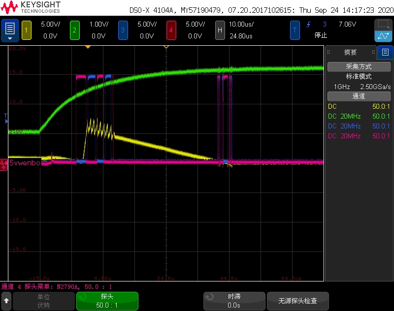
When we did the overvoltage test, we increase the voltage between X7-12 and X7-2 to 650V from 440V. In theory, UC2861 will output several pulses and then shut down the pulse output. And our test waveform is as below:

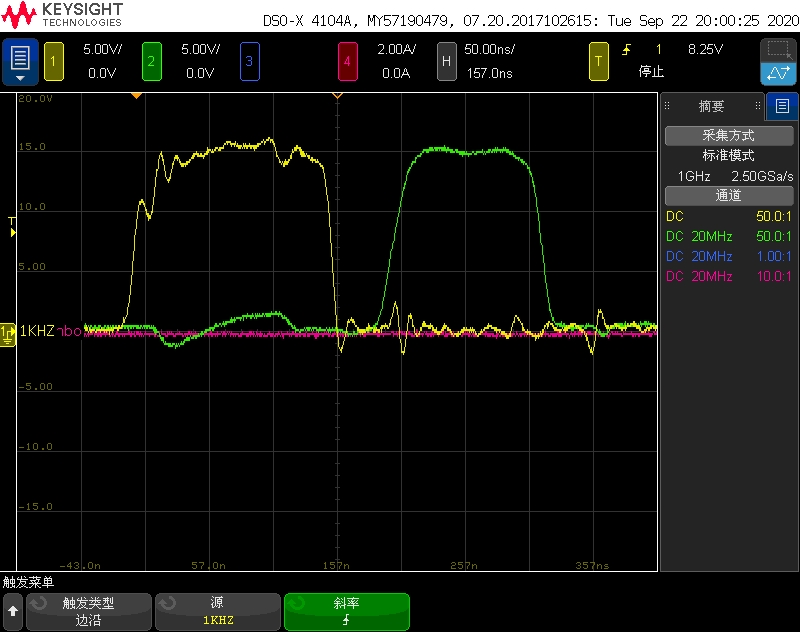
CH1=UC2861's Aout pin. CH2=UC2861's Bout pin. As you could see, Aout and Bout output 3 pulses respectively and then stops. But the first pulse between Aout and Bout has a very short dead time which is not safe to drive the MOSFET. But later the dead time becomes to normal for the second pulses and third pulses.

When we zoon in the first pulses as below picture, we can find the dead time is only 50ns which is too short.

So could you please help advise why the 1st pulse has so short dead time in the over voltage test condition? How can we adjust the circuit to make it normal? Thanks.

Best regards,

Wayne

  • Hi,

    Did you get the pulses before you increase the voltage from 440V?

  • Hi Hong,

    Please refer to below waveform.

    CH1=soft-ref pin.

    CH2=fault pin

    CH3=Aout

    CH4=Bout 1nf波形

    As you could see, when Vin is increased up from 440V, fault pin is pulled to high. Then Aout and Bout output pulses show short dead time.

    If we zoom in Aout and Bout pulses when fault pin is high, we could see the dead time is too short.

    We also tried to change C31(at the left bottom corner in the schematic) value from 220pf to 1nF and we found that the dead time issue can be improved a lot. So could you help advise why C31 value can make the difference?

    Best regards

    Wayne

  • Increase C31 helps to smooth signal to FAULT pin. You may probe FAULT pin to see if the noise on FAULT pin is crossing the FAULT pin threshold so to affect internal circuit, as it looks there is no or very small hysteresis on this pin. So crossing back and forth the threshold may cause internal logic issue and change the dead time.

  • Hi Hong,

    thanks for your reply. One more question from customer is that they used to use UC2861 through hole package device and the schematic is totally the same. But it never shows this kind of dead time issue. When customer changed UC2861 device from through hole package to DW package, the issue begin to show up. So is there any difference between this 2 kinks of UC2861 package device?

    Best regards,

    Wayne 

  • Hi,

    The die/silicon circuit is the same. The through hole package is bigger and DW is much smaller. So there is some difference between packages, such parasitic capacitance, etc. As the two packages are different, the PCB layout is different. I think the PCB layout difference can have much bigger effect and possible to introduce noise to the FAULT pin.