This thread has been locked.

If you have a related question, please click the "Ask a related question" button in the top right corner. The newly created question will be automatically linked to this question.

UCC28730: Diode Snubber

Part Number: UCC28730
Other Parts Discussed in Thread: PMP20634

I am currently Working on a Flyback Converter Design based around the Ti UCC28730 IC.

My first Design is very similar to the Ti PMP20634 Reference Design, it is working how it should.

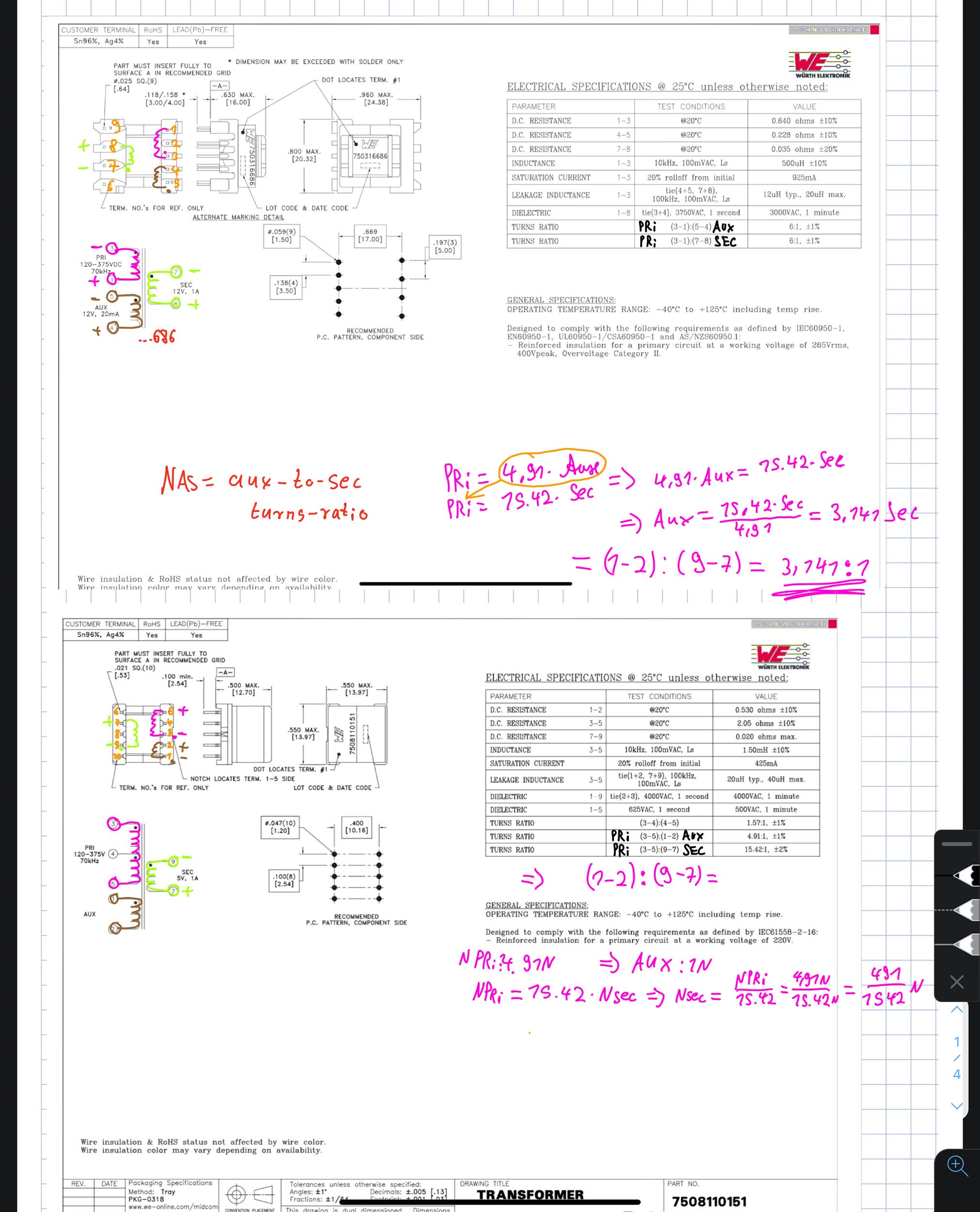
I want to use a smaller Transformer so I changed the WE750316686 to the WE 7508110151. I used the same exact PCB and also changed the MOSFET to a Infineon IPW65R037C6 on both designs, the first Design is still working with the new Mosfet so this should not be the problem.

My Output Voltage on my second design with the smaller Transformer is very unstable and I can only conduct around 3W before the Voltage on the Output drops to zero.

I recalculated all the smaller Resistors for both Transformers, this should also not be the problem?

The picture of the Scope shows the Source Ground Measurement of the circuit with the hot snubber.

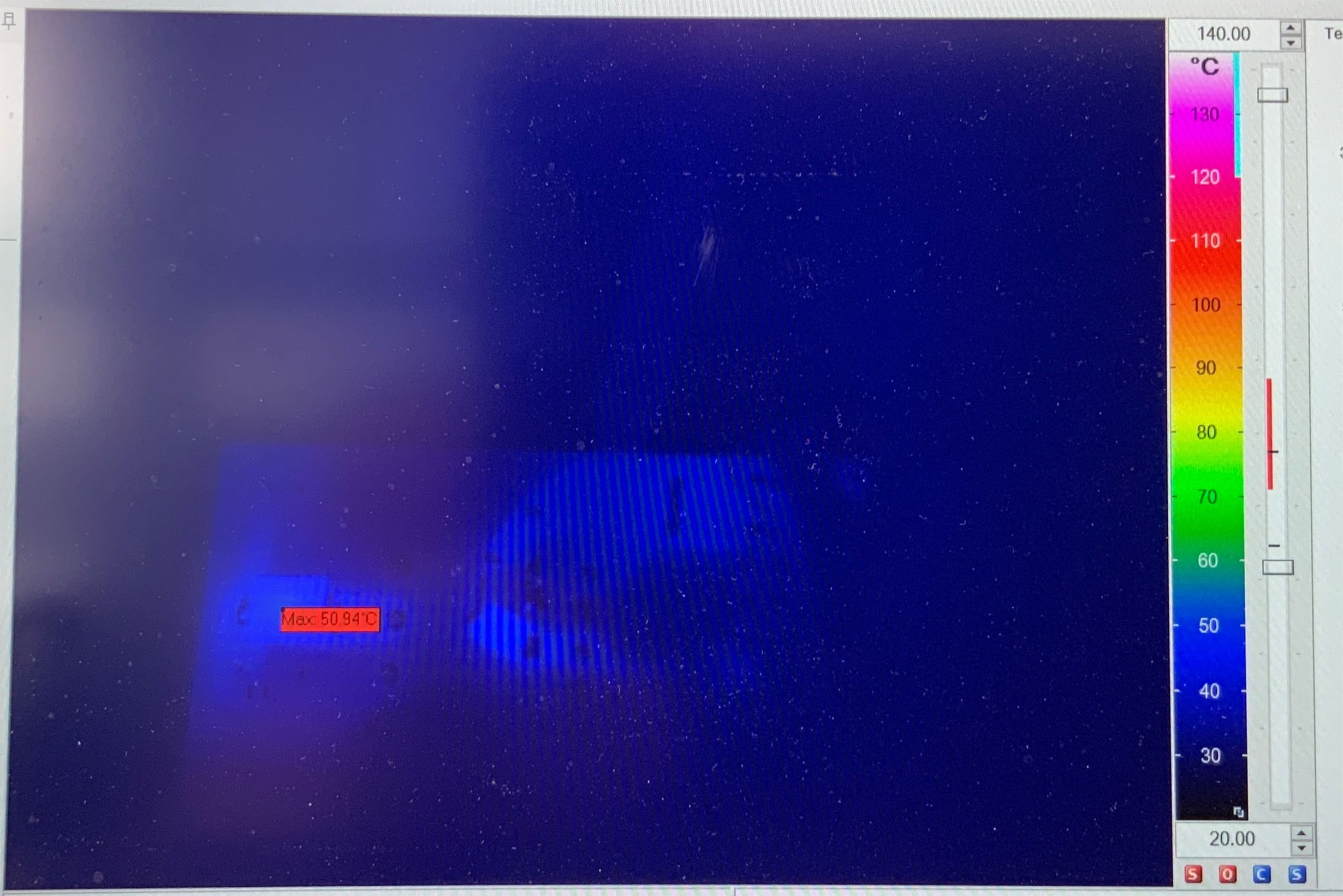
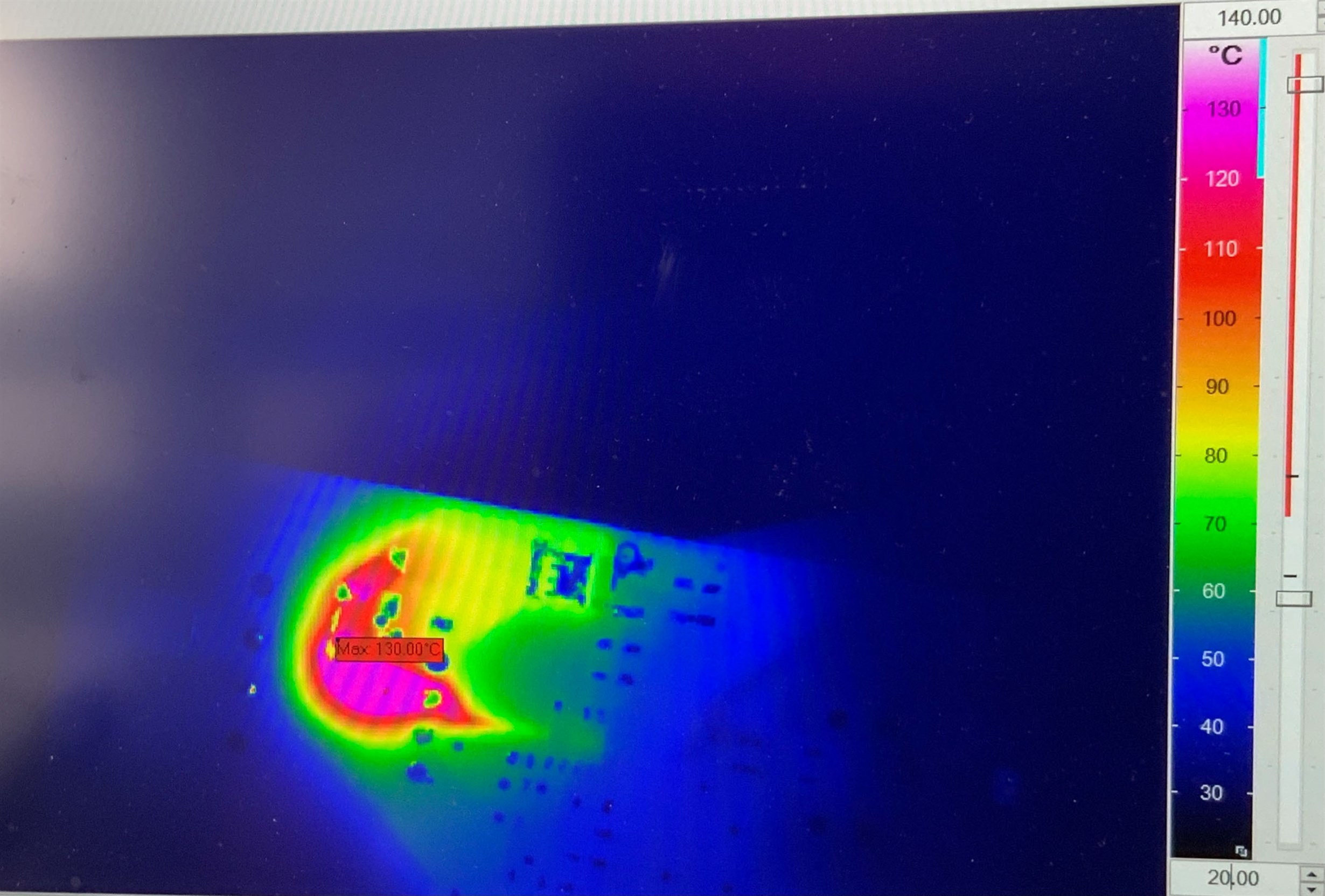
The Thermal Images of the two Boards (Diode D2) reveal that the Diode D2 on the Board with the smaller Transformer (7508110151) is getting very hot, so this should be the main problem.

I am pretty certain that I have to redesign my Diode Snubber, maybe a 200V Diode (currently 150V) would be the solution, is this correct?

What do you think?

Would it be even possible to use no snubber at all because my MOSFET can handle up to 650V?

I would be really thankful for a Solution.

With best regards

Daniel

University of Stuttgart.

  • Hello Daniel,


    Thank you for your interest in the UCC28730 flyback controller.


    The source of the problem is the smaller transformer which has significantly different properties than the original one.   The original transformer Pri:Sec ratio is 6:1, which means that the reflected voltage on the primary winding during the “flyback” interval = 6*12V = ~72V (ignoring output diode drop).


    Assuming that you kept the output voltage the same, at 12V, the smaller transformer has a P:S ratio of 15.4:1, which means the reflected voltage = 15.4*12V = ~185V. This is well above the 150-V nominal rating of the transient voltage suppressor (TVS), D2. Essentially, D2 is clamping the primary voltage and preventing the output from reaching 12V, but more importantly, it is forced to absorb almost all of the energy of each switching cycle. That is why it is getting so hot.

    This clamp (technically not a snubber in this case) is intended to clamp and absorb only leakage inductance energy not coupled to the output winding.

    Raising the rating of D2 to 200V will improve the situation, but still leave the design in a marginal situation because a TVS does not clamp hard at the rated value, it clamps at higher voltage values depending on the peak current going into the TVS.  With 264Vac input + 185V reflected, you get ~558V on the MOSFET drain plus whatever voltage the TVS clamps to. With 650V rating, there is ~92V headroom for the TVS to clamp and still leave some margin to the MOSFET maximum rating.


    All that aside, I believe that changing to 200V for D2 is an immediate, temporary stop-gap solution.

    A true solution would involve redesign of the original transformer for smaller size, if it is possible. The original parameters of primary inductance and turns ratios are determined by the system input and output requirements. Changing any of these will have consequences to the potential range of input or output capabilities. Ideally, you want a smaller transformer with the exactly same inductance and turns ratios as the larger part. Some small deviations may be accommodated, but your substitution is not a small change. It may work in some limited ranges, but not over the full ranges as with the original transformer.


    The UCC28730 design calculator tool (link: https://www.ti.com/lit/zip/sluc579 ) can generate the correct transformer parameters needed to meet all of the specified input and output requirements, regardless of transformer physical size.


    Regards,
    Ulrich