A related question is a question created from another question. When the related question is created, it will be automatically linked to the original question.
If you have a related question, please click the "Ask a related question" button in the top right corner. The newly created question will be automatically linked to this question.
If I understand your question correctly, you are asking if you need to connect load to the TPS65145 output rails to test proper powerup of TPS65145. If so, I do suggest to connect the load to to ensure that all rails power up correctly in your target application.
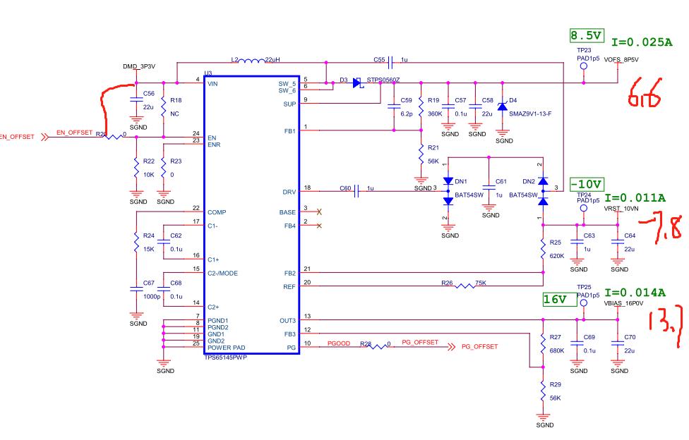
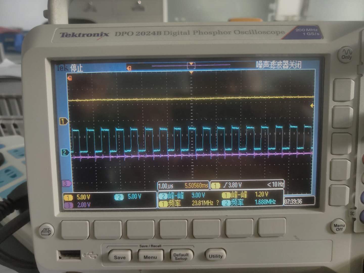
I believe all other voltage rails are incorrect because boost voltage is not at correct level. Schematically, the only thing I can think of is that perhaps some instability because of high 22uH inductor value. Typical schematics recommendation in the datasheet is for 4.2uH boost inductor. Can you please capture Vin, SW node and boost output voltage on same scope plot? Not sure but this may provide some clues as to why you are not getting correct voltage at boost output.
I don't see any particular problem with the waveforms so I am not sure why you are not getting the correct voltage level at the boost output. You may want to have your local TI FAE check your board in the lab to further debug this.
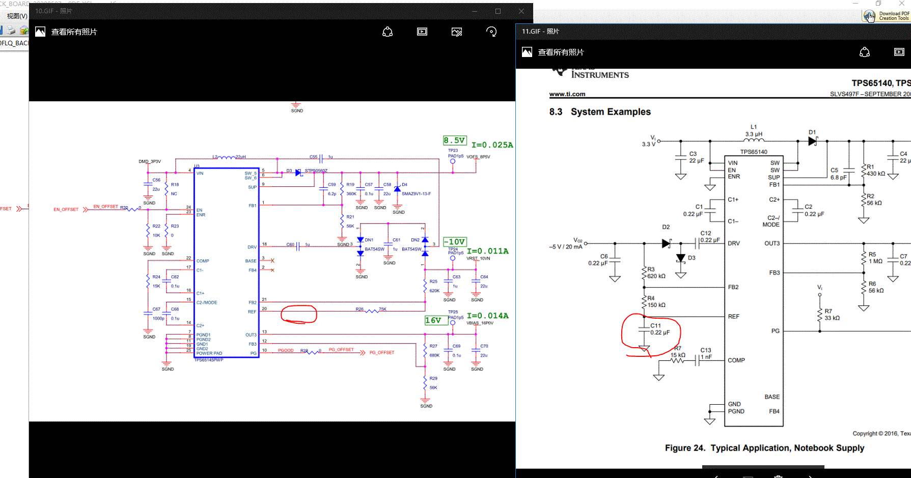
Internal reference is supposed to be at 1.213V nominal. The only thing that I can think of that can cause it to be this low is perhaps negative charge pump feedback network but with R26 at 75K, this should not load the reference. So I would suspect a damaged device. Is this just one board or do you have more than one board with this reference voltage issue?
I am glad that you found the missing capacitor and I somehow overlooked it when reviewing your schematics. I do not know the details of the internal circuit but this capacitor is required for proper operation of internal reference circuit.