This thread has been locked.

If you have a related question, please click the "Ask a related question" button in the top right corner. The newly created question will be automatically linked to this question.

TPS61093: Two steps output voltage

Part Number: TPS61093

HI,

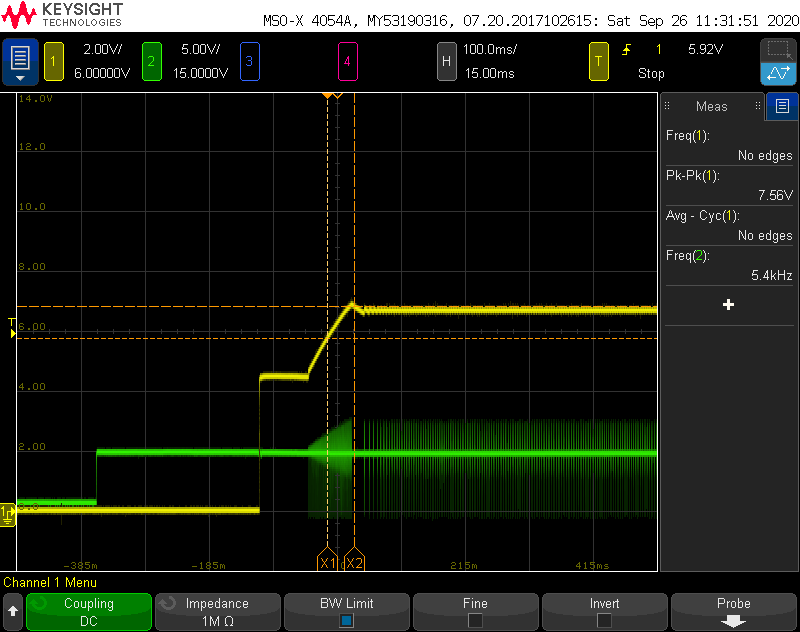
We're using TPS61093 to boost the output voltage to 6.75V.  We can reach 6.75V in the end, but during the ramp-up. we can see a two-step behavior as below.

Please help to explain why there's a two-step behavior like this and if we specify the delay for the period during the first step before SW starts to work.  THanks!

CH1 :VOUT   CH2: SW

Thanks

Antony

  • Hi Antony,

    The device charges the output capacitor to VIN firstly, then the FB pin voltage follows the SS pin voltage until it reaches 0.5V.

    the time that VOUT rises from zero to setting value can be calculated by equation 2 in Startup-up chapter of the datasheet. The VOUT flat period is defined by the ratio between the VIN and setting VOUT. if the VIN is small, the flat period is short; if the VIN is closed to VOUT, the flat period is longer

  • Hi Antony:

    May you share the schematic with us? What's the load during startup?