This thread has been locked.

If you have a related question, please click the "Ask a related question" button in the top right corner. The newly created question will be automatically linked to this question.

BQ25710EVM-017: Low side gate drivers load

Part Number: BQ25710EVM-017
Other Parts Discussed in Thread: PMP40441, CSD17551Q3A

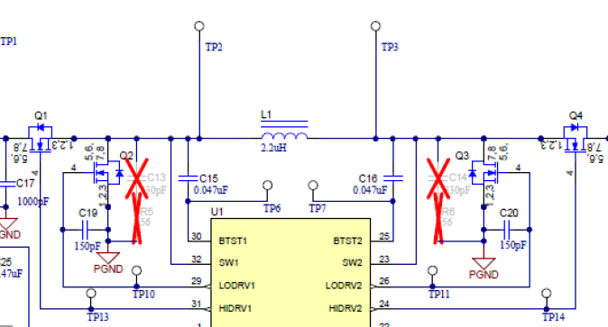
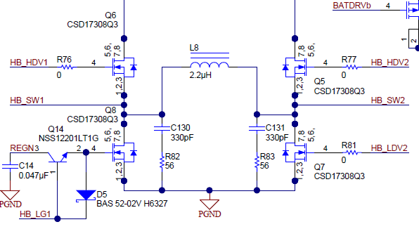
Hi. Can you please explain the purpose of additional 150 pF capacitors (C19 and C20) at the gates of low side MOSFETs? I don`t see anything about it in datasheet and related documents.. In another schematic (PMP40441) there are only one additional circuit at the gate of low side buck transistor and rc-snubbers.  In first case it seems to slow down turn on/off MOSFETs (total gate charge in spec is 6nC plus additional gs capacitance),in second vice versa(total gate charge in spec is 3.9nC plus additional charge/discharge current pump). Thanks!
  • Hi, Alex,

    C19 and C20 are sized to increase the effective Cgs in comparison to the Cgd of Q2. This helps prevent the Miller capacitance from driving the MOSFET gate during a high dV/dt event. This is more important when Qgs and Qgd of Q2 are similar in magnitude.

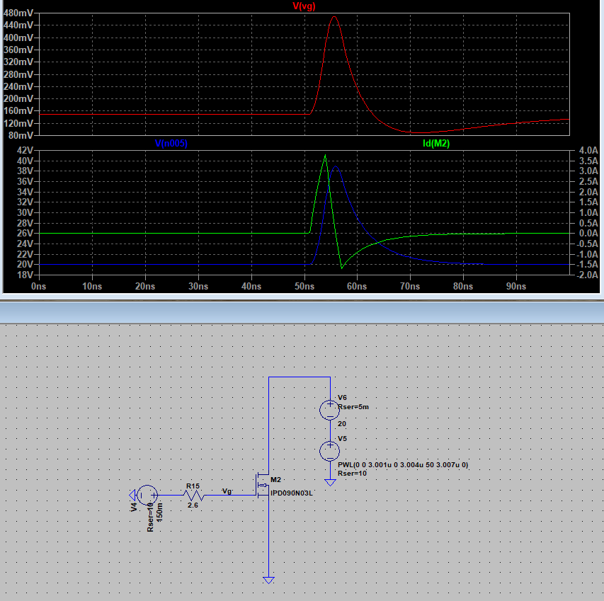
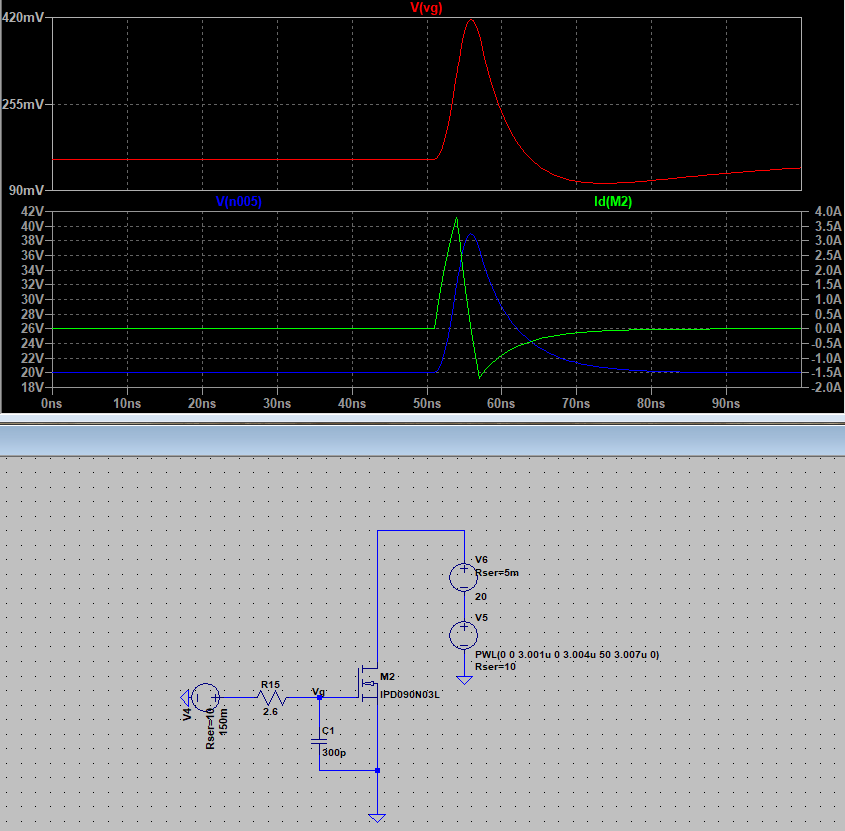
  • Hello Tiger! Many thanks! Can you suggest any related documentation or guide for that issue? As i know Cgs always bigger than Cgd. In related CSD17551Q3A datasheet curve the highest value for Cgd is about 150pF and Ciss is 1 nF at the same time. I tryed to simulate situation with high voltage impulse in spice with IDP090N03L model (Cgs=1.16n, Cgdmax=0.28n) and didnt see any changes with additional capacitor. Maybe i do something wrong with that?

  • Your approach is very good, systematic. They are optional placeholder capacitors.