This thread has been locked.

If you have a related question, please click the "Ask a related question" button in the top right corner. The newly created question will be automatically linked to this question.

TPS54160A: Simulation results and design results are not identical

Part Number: TPS54160A

The voltage that measures between PH and GND is lower from VIN by ~8 volts(On my PCB design). it seems that the drops voltage on the internal MOSFET is high. Running my simulation design on the web site, I get the same voltage as the input voltage(PH to GND). The TPS54160A has an integrated boot regulator that allows the MOSFET gate to be higher from Vin . Can you help me understand the phenomenon I am coming across?
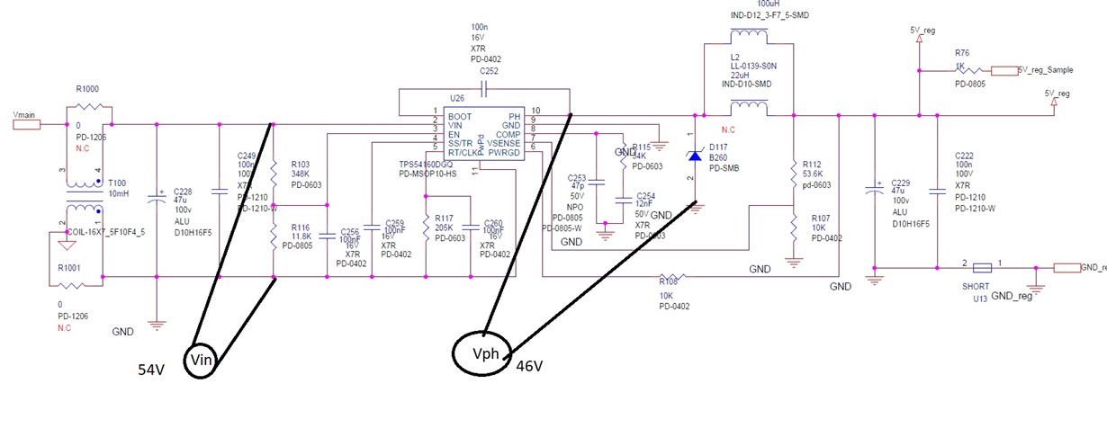
  • Can you share waveform with both Vin and Vph?

    What is loading condition?

    Can you do same waveform with minimal load?

    Thanks.

  • the loads are between 0.1A to 0.5A.

    Yellow - input voltage 54.8V
    Purple- Measured on PH, lower from VIN by ~8 volt

    The voltage that measures between PH and GND is lower from VIN by ~8 volts(On my PCB design). it seems that the drops voltage on the internal MOSFET is high. Running my simulation design on the web site, I get the same voltage as the input voltage(PH to GND). The TPS54160A has an integrated boot regulator that allows the MOSFET gate to be higher from Vin . Can you help me understand the phenomenon I am coming across?

  • Hello

    I am not sure if you still need help with this question.

    However, 8V is a large drop.

    Please be sure the the bootstrap capacitor is the correct value and is soldered in place correctly.

    Also, an 0402 case size is rather small and may be de-rating.

    Please be sure that your scope probes are correctly compensated and your scope bandwidth is adequate to the task.

    Please send a view of your PCB layout.

    Thanks

  • Hi 

    The boost capacitor is correct and I measure the voltage on the cap is around 6~8v. when I removed the boost capacitor, the voltage that I measured on the diode (PH pin) is the same , it seems that the driver of the Mosfet is not working well.

    In BUck's topology, the voltage on the diode while the switch is open is the input voltage.
    With your IC design, I measured voltage, which is lower from VIN by Vgs of the switching MOSFET. it indicates the Boost is not working properly or issue with the MOSFET driver.
    I am trying to understand the problem. Even when I measured the voltage on the switch I got of 6 volts, it shows that the switch did not open to full conduction.

  • Hi

    it seems that the wrong measurement is the result of the prob of the scop that was not calibrated.

    Thanks 

    benny M