Other Parts Discussed in Thread: TMS320F28335, TMS320F28388D, TPS7A11, LP5912, TPS745, TLV757P, TPS746-Q1, TPS7A90, TLV755P, TLV759P, TLV758P, LP5912-Q1, TPS745-Q1, TPS746, , TPS7A87, TLV767, TPS7A25, TPS751, TLV751, TLV752
Our any board is exist inner the servo drive unit used on the industrial machine.
The board is presently composed by TMS320F28335.
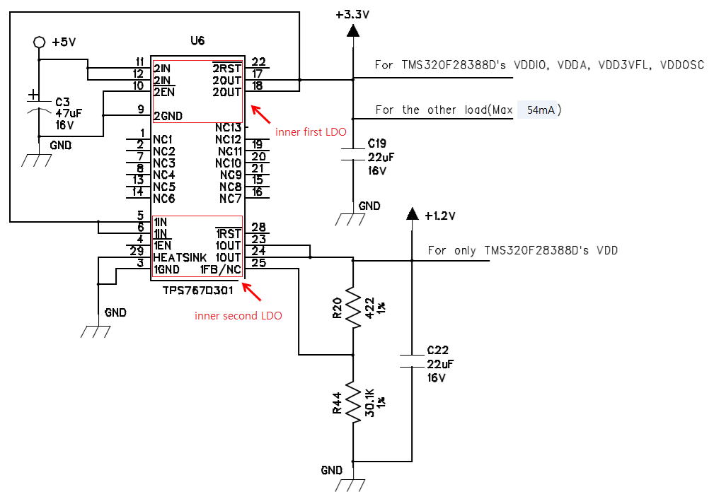
TMS320F28335’s power source is TPS767D301.
5V is applied as the inner 2 channel LDO’s input sources of TPS767D301.
The TPS767D301’s 3.3V output is used for TMS320F28335’s VDDIO, VDD3VFL, VDDA2, VDDAIO and another circuits outside of the TMS320F28335.
The another circuits’ 3.3V current consumption is Max 124mA.
The TPS767D301’s 1.9V output is used only for TMS320F28335’s VDD, VDD1A18, VDD2A18.
I would like to change DSP used on the our board by TMS320F28388D.
And I would like to continuously use the TPS767D301 because we have to use all the many remained TPS767D301 during production of the board after changing DSP.
We wish to use the board up to the max ambient temperature 90℃.
So that, I ask to you questions below. Please I want to receive quick answers from you.
Questions;
1. Is it possible that TPS767D301’s inner first LDO’s output is applied as power source of TPS767D301’s inner second LDO?
If the method is not possible, I want to know the reasons.
2. In 2000 year’s datasheet, the TPS767D301’s minimum output is 1.8V.
But in 1999 year’s datasheet, the TPS767D301’s minimum output was 1.2V.
When I tested, it was possible that 1.2V is outputted from TPS767D301.
I wish to know the reason you announced that the TPS767D301’s minimum output is 1.8V.
3. If it is possible that on the TPS767D301 the its inner first LDO’s output can be the its inner second LDO’s input and TPS767D301 can outputs 1.2V,
I would like to configure as follow.;
For the power source of TMS320F28388D, I supply 5V to the first LDO of TPS767D301 and 3.3V output of the first LDO is connected to the second LDO’s input.
The TPS767D301's second LDO’s output 1.2V of is used for the TMS320F28388D’s VDD.
The TPS767D301's first LDO’s output 3.3V is used for the TMS320F28388D’s VDDIO, VDDA, VDD3VFL, VDDOSC and the another circuits(Max. 124mA).
Is this method is possible? If not possible, I wish to know the reasons.
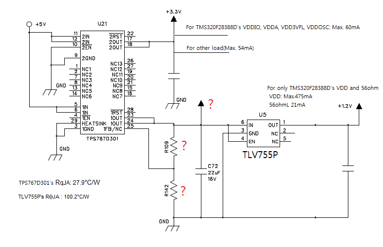
4. Although it is possible that on the TPS767D301 the its inner first LDO’s output can be the its inner second LDO’s input, if TPS767D301 can not outputs 1.2V,
I would like to configure as follow.;
For the power source of TMS320F28388D, I supply 5V to the first LDO of TPS767D301 and 3.3V output of the first LDO is connected to the second LDO’s input.
The TPS767D301's second LDO’s output 1.8 or 1.9V is used as input of the another LDO which outputs 1.2V for TMS320F28388D’s VDD.
The TPS767D301's first LDO’s output 3.3V is used for the TMS320F28388D’s VDDIO, VDDA, VDD3VFL, VDDOSC and the another circuits(Max. 124mA).
Is this method is possible? If not possible, I wish to know the reasons.
5. The 1.2V output LDO mentioned in the 4'th paragraph above was selected as follows.
Is there any problem with selection?
TPS745, TLV758P, TPS746, TLV759P, TPS7A11, TPS745-Q1, TPS746-Q1, TPS7A90, LP5912-Q1, LP5912, TLV755P, TLV757P
WSON6 Package
6. Can the LDOs mentioned in the 5'th paragraph above be used as power source for DSP including TMS320F28388D?
There are colleagues who are concerned about using the LDO mentioned in the 5'th paragraph above because the DSP is not mentioned in the Applications of the LDOs' data sheets.
If the DSP is not mentioned in the datasheet's Applications of any LDO, can't the LDO be used as a power source for the DSP?
If not possible for use, I wish to know the reasons.
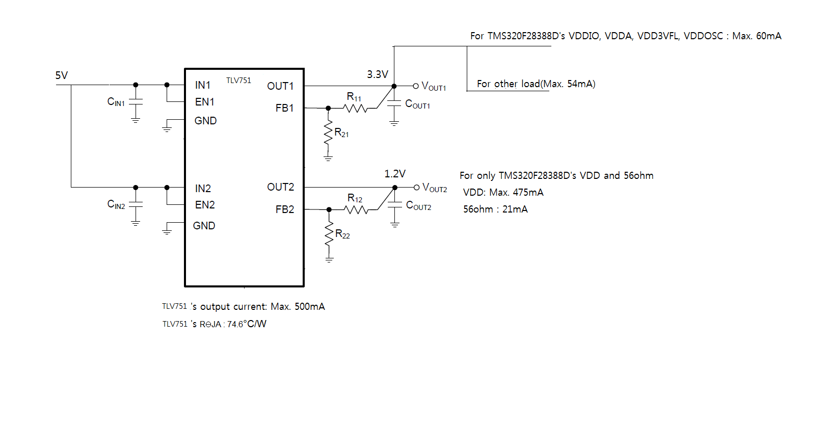
7. After using all he TPS767D301, which is left a lot, we wish to change the design of the DSP power circuit at a lower price.
Would you like to recommend a power circuit for TMS320F28388D that can be used up to 90℃ while having a small number of parts, a small space, a low total price?
Of course, the power circuit should be able to supply up to 124mA to the external circuit of the TMS320F28388D.