This thread has been locked.

If you have a related question, please click the "Ask a related question" button in the top right corner. The newly created question will be automatically linked to this question.

TPS2121: Mux Output Voltage drop during Switchover from Main power to Super Cap Power

Part Number: TPS2121

Hi TI Team,

Good day.

We are facing one issue in our designed circuit with TPS2121 Power Mux.

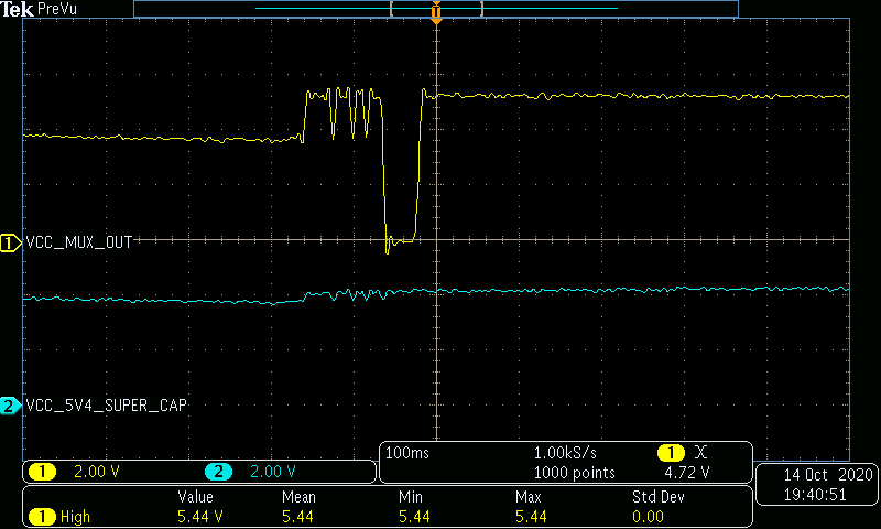
Please find the attached images for your reference

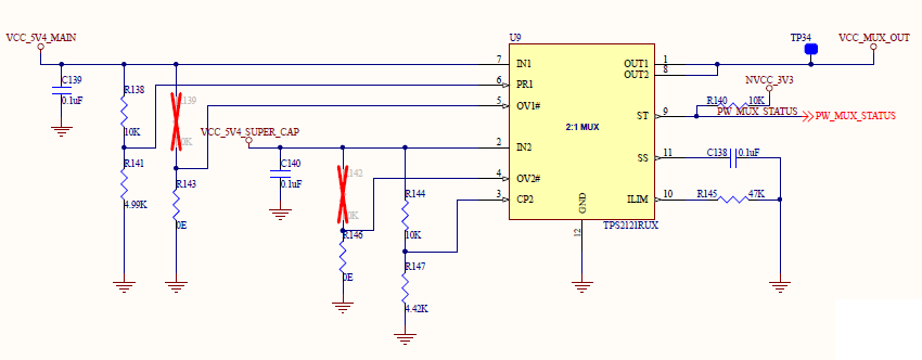
We have used this circuit for Switching from Main power to Super Capacitor for graceful shutdown feature.

The issue is, the output voltage dropping (VCC_MUX_OUT) to Zero while Switching to Super Cap power (IN2). But this problem is happening sometimes only.

Mainly observed this issue while consuming more current like 1Amps through Mux. In low load condition like 400mA, we haven't faced this issue

And also we observed this issue while having load variation in the output.

Please let us know your suggestion, is there any problem in the designed circuit?  Why Mux Output Voltage is dipping?

Thanks & Regards,

Muneeswaran R

  • Hi Muneeswaran,

    I see that in your system you are trying to use fast switchover and the switchover voltage is somewhere around 3.18V. Is this correct?

    When using fast switchover what can happen is that during the instantaneous loading and unloading of the rails, the device bounces between the two inputs as the voltage on the rails rises and falls quickly. This is likely to happen in higher load conditions since the rails will droop and rise more than when compared to a low load case.

    I recommend using the ST pin to add hysteresis. This means that the switchover trigger of IN1->IN2 and IN2->IN1 are slightly differentiated which allows for some small ringing/droop/rise during the fast switchover. Please refer to this tech document for further information on how to implement hysteresis and the physics behind it.

    https://www.ti.com/lit/ug/tidue50/tidue50.pdf 

    Thanks you for choosing TI Power MUXes in your designs.

  • Hi Shreyas,

    In our design, we set the Switchover voltage (Vsw) around 5V. (Please refer the above schematics resistor divider values for calculating this Vsw).

    I don't know, how this 3.18V (Vsw) coming which you mentioned. Can you please tell me If I am wrong?

    I also want to tell few points below.

    1. Issue is occurring randomly, (please find the below graph which is captured during normal switchover from IN1 to IN2)

    2. We haven't faced this issue while both the Power in ON condition. Issue only occurring during Power OFF/ Power ON time of Main Power (IN1)

    Since the switchover is not happening during both the inputs ON condition, and also there is enough threshold available between PR1(1.79V) and CP2 (1.65V). Considering these two points I think adding ST pin hysteresis not required, is that correct?

    Please let me know your valuable suggestions.

    Thanks & Regards,

    Muneeswaran R

  • Hi Muneeswaran,

    1. Apologies, the 3.18V is a typo. The switchover voltage is 4.97V as you stated.

    V_PR1 = 5.4*(4.99/(4.99+10)) = 1.797V

    V_CP2 = 5.4*(4.42/(4.42+10)) = 1.655V

    Assuming, both inputs are available, IN1 is prioritized 

    V_SW (Voltage on VIN1 for switchover to occur from VIN1 to VIN2) = 1.655*((4.99+10)/4.99) = 4.97V.

    2. The point about hysteresis still stands though. This is because the steady state difference does not matter as much as the difference during switchover. When IN1 drops, the voltage on PR1 drops too. As CP2>PR1, the device switches over from IN1 to IN2. Now, IN1 is unloaded and it rises slightly again. All of a sudden PR1>CP2 since the trigger point of switching from IN1 to IN2 and from IN2 to IN1 is the same! The device then tries to switchover to IN1. This process can repeat itself over and over again and with larger load currents, the rails can jump and droops quite significantly.

    If in this situation, IN1 is being removed (or turned off), the amount of energy on this rail is really low which means that if a connection is established, the output will drain the input rail causing the voltage to eventually drop below UV. Once the device hits this stage, it will recover with slow switchover, with settling time and with soft start rise time to IN2 (as you have seen).

    The goal of hysteresis is to change the switchover points. For example, if we were to redo the situation as describes as above, IN1 falls and the switch transitions to IN2. VIN1 is unloaded and rises as expected. BUT the major difference here is that the resistor divider network has changed and so the transition voltage is higher. So the instantaneous jump on IN1 is insufficient to cause the device to switch back to IN1. This is why even a small change of resistor divider network while switching can lead to more reliable and robust transitions especially in fast switchover mode.

    I hope this detail has made the situation clear.

    Thank you for choosing TI Power MUXes in your designs.

  • Hi Shreyas,

    Thanks for your detailed answer.

    I will check with our setup and let me update here as soon as possible.

    Regards,

    Muneeswaran R

  • Hi Shreyas,

    We have added 100K resistor between ST and PR1 pins for adding Hysteresis.

    After this change we have not found any reboot issue (voltage drop to zero) while switching from IN1 to IN2.

    But still we are facing some issue while switching from IN2 to IN1. But it is happening only with high load condition (Approx 1.4Amps).

    Please find the below image for your reference.

    Can you please provide your suggestion?

    Thanks & Regards,

    Muneeswaran R

  • Hi Muneeswaran,

    Good to hear that the hysteresis has helped a bit.

    Could you retest this event at a smaller time scale and take the following two scopeshots

    1. Measure V_in1, Vout, V_in2 and I_out

    2. Measure PR1, CP2, ST ->please set the GND of PR1 and CP2  waveform as the same. This will help us see if and when the switchover takes place

    I am suspecting two different possibilities. Either the issue is once again brought about by the recovery of the super cap or there is an inrush spike that causes the device to current limit and fail eventually.

  • Hi Shreyas,

    We have found some voltage dip issue in the Main input power supply (IN1). This is happening while IN1 voltage rising (Switching from IN2 to IN1).

    After that we increased the Power supply current limit (to manage high load current during switching at voltage rising), then we have not found voltage dip during switching from IN2 to IN1.

    This is working for us. Thanks for your valuable support.

    Regards,

    Muneeswaran R