This thread has been locked.

If you have a related question, please click the "Ask a related question" button in the top right corner. The newly created question will be automatically linked to this question.

LM5050-2: Inquiries related to poor output

Part Number: LM5050-2

Hi, TI expert

I have an inquiry while using the LM5050-2 (LM5050MKX-2/NOPB) by a customer.

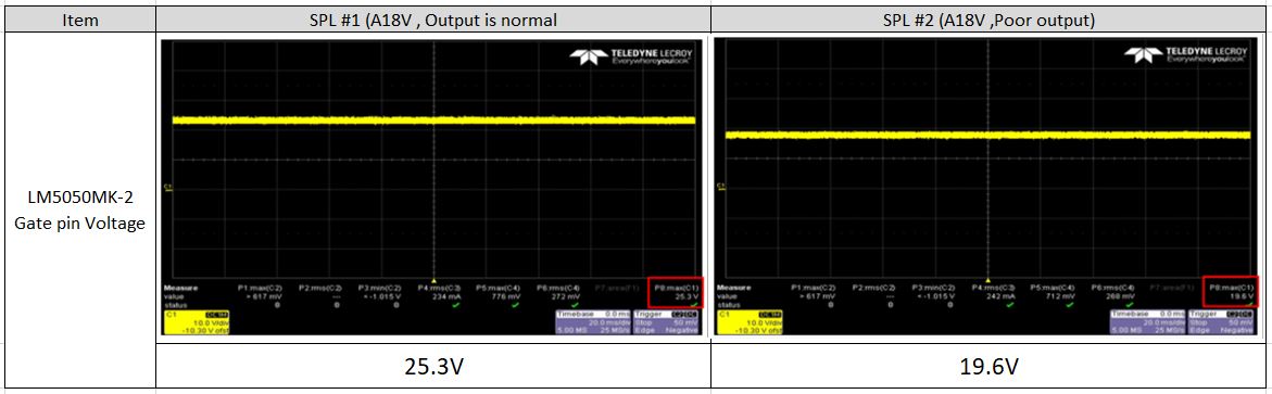
  * A18V output is normal after replacing defective IC

1. Symptoms

There is a phenomenon in which the output is dropped by 0.8V compared to the FET input. (Vin: 18V → Vout: 17.2V)

2. Review items

-Check the difference by about 5.7V when reviewing the IC Gate Pin Level (Good: 25.3V / Bad: 19.6V)

-Output is normal when bad board, gate pin pattern is cut off and DC voltage 25V is applied

-Same phenomenon occurs when bad IC is swapped to a good board

Please check the above 1. Symptoms and 2. Review items.

Thank you.

  • Hi Leo,

    The  behavior of the LM5050 regulation loop is as follows:

    1. If Ron * load current is > regulated forward threshold, gate voltage increases (up to the charge pump voltage)
    2. If Ron * load current < regulated forward threshold, gate voltage decreases (until Ron * load current = regulated forward threshold)
    3. If Ron * load current is < reverse current threshold, gate pulls down quickly

    This behavior is explained clearly in section 'IN, GATE AND OUT PINS' of datasheet.

    For a input voltage of 12V and above the Gate voltage should be around 11V greater than input voltage when the load current is high (Iload*Ron>Regulated Forward threshold).

    If the load current is less, the gate voltage is regulated to a value less than 11V (Vgate-Vin).

    • Please share the schematic for review.
    • Are there any tests that you have done on the system. This is to understand  the probability of IC being damaged due to any tests.

  • Hi, Praveen

    Customers are reluctant to disclose schematics.


    If you provide your personal email address, we will share the schematic by email.


    Reply please.

  • Hi Leo,

    You can send a friend request to me on e2e and once we are friends we will be able to share documents privately. 

    Meanwhile, can you let us know if any tests are performed on this device which can potentially damage it ?

  • Hi, Praveen

    I requested a friend. (To share the schematic)

    Also, there was no test that could damage the device.

  • Hi Leo,

    I have got you friend request and I have accepted it. Let me look into your comments and get back to you within couple of days. 

  • Hi, Praveen

    Regarding the last time'M5050-2: Inquiries related to poor output', I sent a schematic with a message.

    When can I get a reply?

    Customers want quick answers.

    And, if possible, could you please reply with my e-mail?

    E-Mail: leo.lee1@arrow.com

    Thank you.

  • Hi Leo,

    From your description it looks like the device is damaged. 

    Did the IC initially work as expected and then stop working ? If yes, after what condition have you seen the drop in Gate voltage ?

    The most common reason for damage of IC's we see id electrical over stress. 

    Generally we recommend a Schottky diode at the output and a TVS at the input to protect the device from transient voltages if there is inductance in the path. More details are in section  '8.1.2 Short Circuit Failure of an Input Supply' of the datasheet.