This thread has been locked.

If you have a related question, please click the "Ask a related question" button in the top right corner. The newly created question will be automatically linked to this question.

ISO5852S: TIDA-00195 : Global shutdown and IN+ signal for the gate driver

Part Number: ISO5852S
Other Parts Discussed in Thread: TIDA-00195

Dear sir,

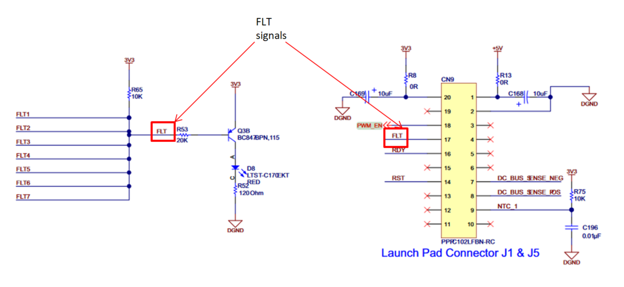
We wish to design the inverter using ISO5852S similar to TIDA-00195.

In this model, all the six FLT signals are connected together and using one 10kOhm pull-up resistor. 

Kindly help us to solve the below queries. 

1. When we connect all the FLT signal with IN+, it drops the FLT output voltage during normal operation. Its recommended to use the logic gate between the FLT output and IN+. Whenever fault is identified in any one of the gate driver, we wish to turn off all the drivers. Shall we use 8 input logical AND gate IC (6 inputs from FLT signals and connect VCC to remaining two inputs.) Could you please suggest the suitable AND gate IC from TI for this application.?

2. Do we get global shutdown option in the TIDA-00195 circuit? 

3. Cloud you please suggest some 5V buffer circuit compatible with ISO5852S 

4. We are using NXJ2S2405MC DC converter to give the 5V power supply to gate driver. The maximum load current is 400mA. Could you please confirm whether it can handle 6 gate drivers ?

Thanks & regards,

Rajasekaran.

  • Hello Rajasekaran,

    Thank you for the interest in the ISO5852S. Our expert on this device is out of the office at the moment but will respond to your questions shortly.

    Regards,

  • Hi Rajasekaran,

    I will be out of office the next few days and will also need sometime to review this. I can get back to you with an update late next week. Would that be okay with your timeline?

    Best regards,

    Andy Robles

  • Dear sir,

    we are waiting for your reply. Kindly update the same.

    Thanks & Regards,

    Rajasekaran.

  • Hi, Rajasekaran,

    Andy is still out. He will get back to you by the end of the week.

    Thanks for your patience.

  • Hello Rajasekaran,

    Thank you for your patience!

    Since there are different questions I will go ahead answer them by parts.

    1. For an AND gate implementation you will need six 2-input AND gates, one for each driver. in this configuration all FLT pins can be connected together and will turn off all the gate drivers in the event of any gate driver outputting a FLT. Refer to the example show below.

    Additionally, one pull resistor is enough for all 6 FLT pins, but each gate driver will need it's own capacitor close to the FLT pin for better noise immunity.

    2. The global shutdown feature in the TIDA-00195 circuit is achieved through the micro-controller. All of the FLT signals are tied together and are sent to the micro-controller. The micro-controller will then receive the FLT signal and depending on the program can disable the PWM signals.

    3. For the input buffer I believe you mean the AND gates for the inputs. Please refer to the AND gate portfolio on TI.com.

    Please let me know if this is not what you meant.

    4. The VCC1 pin of the ISO5852S has a 4.5mA max quiescent current spec. 400mA will be more than enough to power the low voltage input supply of all 6  ISO5852S.

    Let me know if there's any additional questions!

    Best regards,

    Andy Robles

  • Dear sir,

    Thanks for your detailed reply. 

    We will use HD74LS08 AND gate to achieve the globe shutdown in the circuit. 

    How much current does it required in the IN+ for PWM input terminal and shall we use the one qty of NXJ2S2405MC DC converter (5V, max load current 400mA) to provide common 5V power supply to six qty of ISO5852S gate driver and 2 qty of HD74LS08 AND gate. 

    Also cloud you please share your email to send the overall schematic for verification. 

    Thanking you.

    Thanks & Regards,

    Rajasekaran.

  • Hi Rajasekaran,

    The IN+ pin of the ISO5852S is a high impedance pin with a typical leakage of 100uA typical when asserted high. One NXJ2S2405MC should be enough to power the low side of all six ISO5852S gate drivers and both AND gate IC's.

    For the schematic review I have sent you a message with my contact info. Feel free to reach out so I can assist in reviewing your schematic.

    Best regards,

    Andy Robles