Hi E2E,
Would like to know below about power stage:
1. Is there any power sequnece requirement for REFIN(~1.7V), VDD(5V), PVDD(5V) and VIN(12V)?
2. How can host device(such as controller) judge which fault type it is, among OTP and other faults? I see all of them will behave to pull up TAO pin to 3.3V.
3. When powered on, how will TAO pin behave? From 0V to room temperature calcualted voltage?
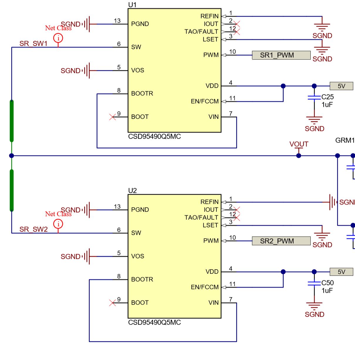
4. If you see from reference design --- PMP22519, CSD9k power stage is used in LLC topology as SR.
As what I learned, IOUT is designed for buck topology operation, which means it will emulate buck inductor current, but in LLC, the current flowing through SR is sine-wave, so IOUT cannot correctly output sine-wave, right?