This thread has been locked.

If you have a related question, please click the "Ask a related question" button in the top right corner. The newly created question will be automatically linked to this question.

UCC28704: UCC28704 switches on and off continuously

Part Number: UCC28704

Hi,

I designed a flyback converter with the UCC28704. I am using the transformer 750811613. The output of the converter should provide one output of 12V and 1 output of 5V while the auxiliary output should be 20V. Unfortunately, the converter malfunctions. In particular, It swiches-on but and after 3 cycles, the auxiliary voltage jumps by 10V. Afterwards, the controller sends small pulses with very high frequency to the mosfet, until the system is led to overvoltage and swithces-off. In the following link you can find a .psdata file with the results. The output capacitance is 330uF.

Blue: Vdd

Red: Voltage on the source of the Rcs

Green: Voltage on the anode of the auxiliary winding diode

Yellow: Voltage on the anode of the 5V output diode

www.dropbox.com/.../ti1.psdata

Best regards,

Gerasimos

  • Hi, 

    I've assign expert of UCC28704 to support you, please wait for the reply.

    BR,

    Yunsheng

  • Hi, Gerasimos,

    Sorry, I can't download your test waveforms through the link you shared , Could you please directly attach the waveforms in the post.

    Thanks.

  • Hi Jaden,

    Sorry for that. In this post you can find the test waveforms. The 'General_waveform.pdf' has the waveforms of one switch-on to switch-off cycleof the IC. Inside this pdf, you can see marked inside cycles the areas which are shown to the other pdf files. In particular, in the 'Rise_of_Vdd.pdf' you can see how the Vdd jumps by 10V after the first 3 cycles and in the 'High_frequency_modulation.pdf' you can see that the IC sends repetitive short pulses to the mosfet in very high frequency, which is theoretically impossible by this chip, leading the outputs to overvotlage, until it switches-off and the sequence repeats.

    Blue:Vdd

    Red:Voltage on Rcs

    Green: Voltage on the drain-source of the mosfet

    Yellow:Voltage on the anode of the 5V output diode

    General_waveform.pdf

    Rise_of_Vdd.pdf

    high_frequency_modulation.pdf

    Best regards,

    Gerasimos

  • Thanks for the waveforms.

    Could you please also share the schematic and let me know your test condition , such as input voltage and output load. Thanks.

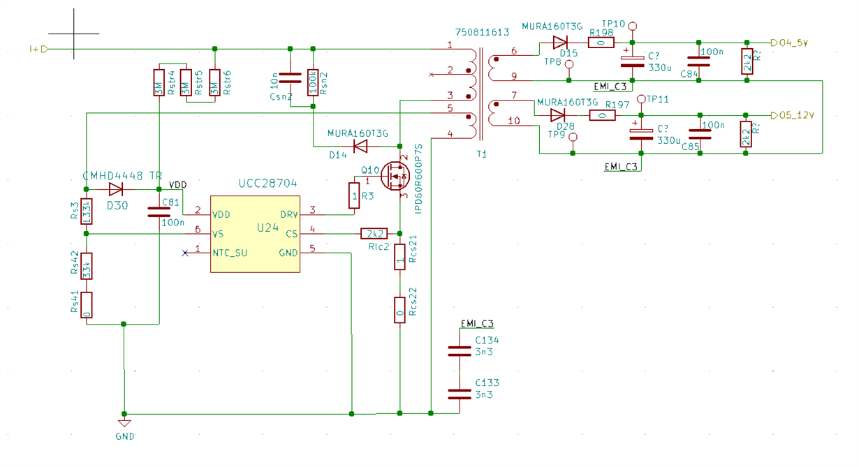
  • In the png file you can see the schematic. Regarding the input voltage it was 280V. In the output I had connected a load of 220 Ohms to the 12V output. The 5V output supplied only the preload resistor of 2k2 Ohms. I ve also tried with different configurations putting load to the 5V output, with the same result. Also I send you another waveform 'Vaux_diode.pdf' which shows:

    Blue:Vdd

    Red:Voltage on the anode of the auxiliary diode

    Green:Votlage on the drain of the mosfet

    Yellow: Output voltage of 5V

    From what I see in this graph, in the red line (Voltage on the anode of the auxiliary diode), the voltage spike on the auxiliary winding because of the leakage inductance is enough to charge the Cdd to much higher voltage than the Vo*Na/Ns, like the IC is not drawing any current from the Cdd. 

    Vaux_diode.pdf 

    Best regards,

    Gerasimos

  • Hello Gerasimos,

    In your "high frequency modulation" waveform , the switching frequency is up to ~160khz which is higher than maximum frequency of 85Khz . that possibly this part misses a sample during a given switching cycle , it will speed up the internal timer to increase the chances for taking VS sample.

    The problem maybe a degraded VS signal , possibly due to excess node-capacitance on VS node due to poor PCB layout , if that's true . two suggestion as below:

    1. Parallel one 1~2pF capacitor on Rvs1 (Rs3 in the schematic), if it works , note that this is only a temporary solution , Ideally , the PCB should be improved : VS pin divider resistors should be placed as close as possible to the controller , should not have ground plate under the resistors and VS pin trace.

    2. If No 1 proposals not works , flying Rvs1 ans Rvs2 (Rs41+Rs42, combine two resistor into one), and let them close to controller.

    Thanks.