This thread has been locked.

If you have a related question, please click the "Ask a related question" button in the top right corner. The newly created question will be automatically linked to this question.

TPS62402: TPS62402 - Converter 2 (3.3V) still active even if EN2 is low?

Part Number: TPS62402

Hello all,

I am struggling with a weird behavior on all of my 4 Testboards including a TPS62402 step down converter to provide me with 3.3V and 1.8V for my peripherals.

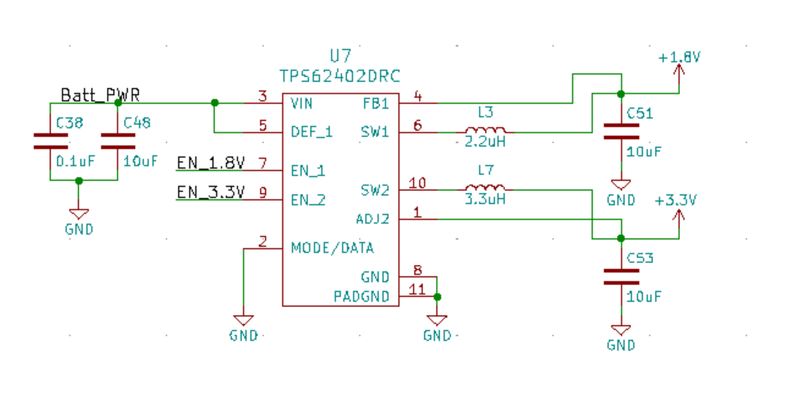
My hardware setup looks like this:

- host MCU Nordic nrf52 (directly powered through the battery)
- TPS62402
- VLSI VS1063 (powered through the TPS with 1.8V and 3.3V)
- SD Card (powered through the TPS with 3.3V)
- RTOS mbedOS

When I am pulling EN1 and EN2 up I am getting the desired 1.8V on Converter 1 and 3.3V on Converter 2. All fine so far but when I am pulling the EN pins down I am getting the following results:

- EN1 (measured on the TPS 0.01V) -> Converter 1 is OFF (output 0.0V)
- EN2 (measured on the TPS 0.04V) -> Converter 2 is still providing output between 1.765V and 2.65V measured on Pin 10.

I could not find any explanation in the datasheet. First I thought it might be a hardware issue related to some other part leaking voltage into the 3.3V rail so I have tried another one of my custom test boards with the same result. I have the same behavior on all of my boards that include the TPS62402. 

My second attempt was to make sure that no other device is providing any current through the (battery powered) host MCU pins so I set all PINs as input and pulled them low. With this approach I am still reading around 1.375V on the TPS converter 2 output.

Is there any obvious explanation that I am missing why I can still measure the mentioned voltage on the TPS? I refuse to believe that all parts are defective. I have attached the schematic part including the TPS62402 hoping that the solution might be obvious.

Thank you already for any hint/help.

Best

  • Hi,

    I am working on your request and will give you a feedback by tomorrow.

    Regards,

    Febin

  • Hi,

    I reviewed the schematic and it looks fine.

    At the moment, I do not know the cause for this observation. It should be that when EN is low the converter should be turned off.

    Could you please capture Vin, Vout, SW and EN pin plots during start up and power down. 

    What is max load on the two outputs?

    If possible we can also look into the complete schematic and layout to analyze further.

    Regards,

    Febin

  • Hi Febin,

    thank you very much for taking the time and looking into this issue and also for reviewing the schematics. If the schematics are looking fine I need to check the hardware one more time. I have figured out that by simply removing the SD card when EN is low, the "leak current" on the converter drops to about 1.2V. As I can not explain this phenomena I assume it might be either a board hardware/design issue (which would be bad as on all 4 boards the same issue exists) or something else.  

    To answer your questions:

    These are the measures for the mentioned Pins on startup/power down:

    VIN VOUT1 VOUT2 SW1 SW2 EN1 EN2
    STARTUP 3.99V 1.83V 3.36V 1.83V 3.36V 3.31V 3.31V
    POWER DOWN 3.99V 0.03mV 1.768V 15.1mV 1.768V 0.00V 0.00V

    The absolute max. load on the converter will be:

    25mA for Converter 1 (1.8V circuit)

    415mA for Converter 2 (3.3V circuit) - typical load will be around 250mA with all peripherals ON and running,

    Best,

    B

    PS: I am happy to share the complete project schematics on a private channel. Just let me know. Thank you for your understanding.

  • Hi,

    I have sent you a private message and we can discuss further internally.

    Regards,

    Febin

  • Hi,

    As we are discussing this issue through private messaging, I will go ahead and close the thread. I hope you will be fine with this.

    Regards,

    Febin