This thread has been locked.

If you have a related question, please click the "Ask a related question" button in the top right corner. The newly created question will be automatically linked to this question.

DCR010505: DCR010505:DCR010505 has failure with no output

Part Number: DCR010505

 HI,

I'm using DCR010505U to generate a isolated 5Vout with a 5Vin.But we found some failure issues.

Some DCR010505U has no output, the fail rate is 2~3%;

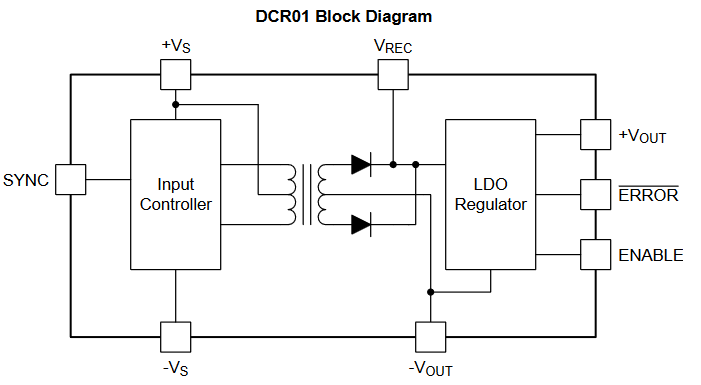
The input voltage for the normal DCR010505U is about 5.05V, then the Vrec pin is about 6.97V, the output voltage is about 4.98V.

I was wonder about the voltage on the Vrec pin,does about 6.97V is the right voltage?

The schematic is showed as below, Whether need add dummy resistor to have a "preload" at the output?

We test the failures DCR010505U,the results is showed as below, it seems like the inner LDO failure or the diode is damaged,

Would you give me some possible influencing factors?

  • I have another question,does the inductor L2 at the output of DCR010505U have some bad effects?

  • Hello,

    We will review the schematic and provide some comments.

    Cheers,
    Denislav

  • Hello Xiao,

    I reviewed the schematic provided and it looks fine. The circuitry seemed to follow the typical schematic on Figure 27.
    The voltage you are reading on Vrec is correct and I don't think a resistor at the output as a "pre-load" is necessary. The device has an LDO internal to keep the voltage in regulation.

    I don't see a problem with L2 inductor placed at the output. Adding second-stage filter is an effective way to reduce output voltage ripple.

    Can you provide more detail on the application?
    I noticed that U3 is stepping down 24V to 5V which supplies the input to DCR01 device (U4). Have you tried to isolate the circuit to only U4 and power it up with an external stable 5V power supply?

    Regards,
    Alejandro

  • HI,Alejandro

    Thank you for your response.

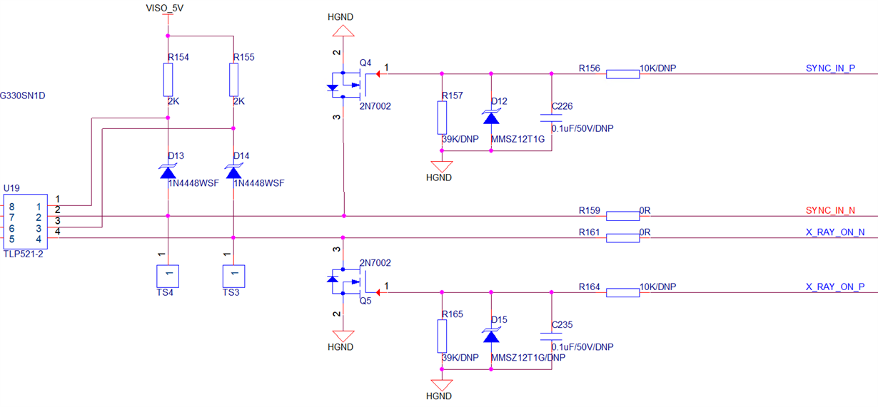
    The output of DCR01(U4) is only used to supply U19(optocoupler).

    The signal sync_in_n is an external signal,segregated by U19 to inner circuit.

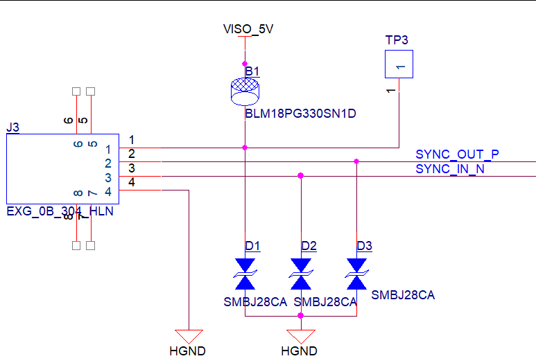
    The sync_in_n and hgnd will connect to an external high voltage generator,2 ~ 3% failure(DCR01 has no output) rate is occured at OQC process

    During OQC process,there may be hot plugging situations,that is during DCR01 U4 is normal output,connect the sync_in_n and hgnd to external high voltage generator

    So associated with outside is sync_in_n and hgnd,do you think introduce interference from hgnd is a possible factors?and how to prevent it?

    As U3,the board is old design,about all upload schematic parts (U3 U4 U19 J3 parts),we keep same the SCH and PCB design with old design.

    It's confused that there is no failure on old product,even if there also may be hot plugging situations during OQC process on old product.

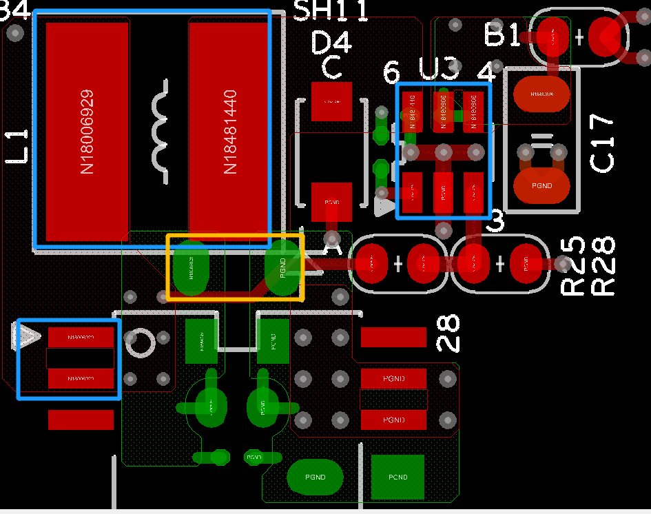
    In addition,the U3 and U4 is not ideal layout,all the capacitor(C21 C19 C20 C27)are at bottom layer, L1 connect the U4 input at top layer,does this will induce failure?

    Thank you again.

  • Xiao, thanks for the information.

    I have a few follow up questions that I would like to get a clarification on:

    1. Can you tell me more about the external voltage generator?
    2. I'm not familiar with the term OQC. What does that stand for?
    3. I'm getting confused on the application. Lets make sure I'm understanding correctly:
      1. Old PCB board design with DCR01 are not experiencing any failures even after hot swap
      2. New PCB board design with DCR01 are experiencing failures only after hot swap.
        Did I understand this correctly?
    4. Even though it's not an ideal layout, I don't believe this will cause such failures.
      The layout we recommend to follow is located in that datasheet, under Layout Guidelines.

    Regards,
    Alejandro

  • Alejandro,

    Thank you for your response

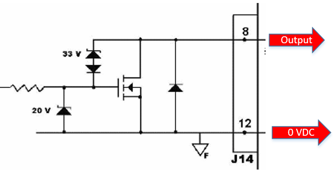
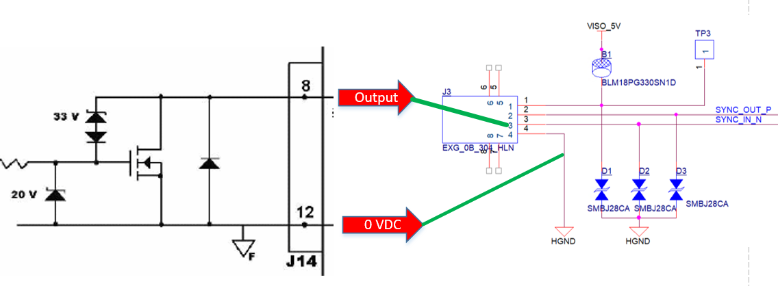
    1.External voltage generator output digital signals,the interface circuit showed below:

    2.The OQC is Out going Quality Control,including fuction、performance、reliability test and so on

    3. a.Yes,old PCB board design with DCR01 are not experiencing any failures even after hot swap

    hot swap just bring in sync_in_n and hgnd,the whole connect showed below:

    b.New PCB board design with DCR01 are experiencing failures,we don't know when the failure happen,

    we also don't konw what causes the failure,hot swap is just one of our suspicion.

    Thank you again

  • Xiao,

    Understood; lets begin by comparing the PCBs.

    You mentioned that the old and new PCB design do not have any differences? How so? So what makes it a new design? BOM change?

    So, the power circuitry is as followed:

    1. U3 to U4 (24Vin to 5Vout)
    2. U4 to U19 (5V to 5V)
    3. U19 connects to J3
    4. J3 connects to an external voltage generator (hot swap)

    Thanks,
    Alejandro

  • Alejandro:

    About all upload schematic parts (U3 U4 U19 J3 parts),we keep same the SCH and PCB design with old design.

    The main differeent between this two design is the size of PCB and external connection.

    The difference didn't effect the U4,because U3 is only supply for U4,U4 only supply for U19.

    That is,from U3 to J3 is a whole part, for this whole part,the old and new PCB design do not have any differences.

    Yes,the power circuitry your described is right.

    Thank you again.

  • Xiao,

    Thanks for the information.
    It's coming to my attention that it might be in regards to your new external connector. When you indicate "external connection", you are referring to the high voltage generator, correct?
    You mentioned that the failure rates begin during OQC process.Are there any changes in the OQC process from previous to new? Any new test conditions?

    Thanks,
    Alejandro

  • Alejandro:

    External connector isn't refer to the high voltage generator; 

    From U3 to J3 is a whole part,J3 connect to the high voltage generator also is the same to the old design; 

    External connector is refer to the different number of sensors,which isn't effect the U3-->J3-->high voltage generator; 

    We don't know when the failure happen,only when this function(high voltage generator output the sync_in_n signal) is detected,

    The CPU can't detect the signal,then we find the U4 haven't output.Function test is one of OQC process.

    The operation of this functional test is also the same with old design.

    We also try to find the difference between the old design and this products,

    Until now,we haven't find which factors will effect the U3-->J3-->high voltage generator.

    Thank you again.

  • Xiao,

    Thank you for clarifying.

    Is it possible for you to share the layout? I'm still concerned on why this phenomena is occurring when no changes where made in schematic or layout.
    If you don't feel comfortable sharing such design here in the forum, we can take this discussion offline. May we contact you at the email address you provided in your E2E profile?

    Thanks,
    Alejandro

  • Alejandro,

    Thank you for your attention,We can take this discussion offline.

    The email address provided in my E2E profile is valid,we can discuss through email.

    Thank you again.

  • Alejandro,

    I haven't receive your email,and I don't know your email address,

    Would your send me email to take this discussion offline?

    Thank you again

  • Hi Xiao,

    Apologies on the late reply. Texas Instrument's was on a national holiday since November 26th.

    I have reached out to you via email. I will close this thread and continue to help you offline.

    Regards,
    Alejandro