Hi All,
I have a question about TPL7407L.
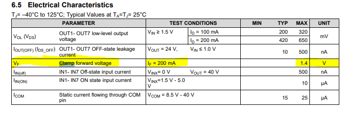
Are there any restrictions on the relationship between COM pin and OUTx pins?
Conditions: COM = 8.5V / OUTx = 40V
Does it work properly with the above input voltage?
Do you need COM=OUTx or COM>OUTx conditions?
Best Regards,
Ishiwata