This thread has been locked.

If you have a related question, please click the "Ask a related question" button in the top right corner. The newly created question will be automatically linked to this question.

TPS2663: TPS2663 and DRV pin under-specified

Part Number: TPS2663
Other Parts Discussed in Thread: STRIKE, CSD19533Q5A, CSD16301Q2

Hello!

Regarding the TPS2663 I think that the DRV pin is under-specified.

The datasheet specifies the following Electrical Characteristics:

TPS2663 Electrical Characteristics - B_GATE (BLOCKING FET GATE DRIVER)

Further down it lists the BSS138 as the MOSFET to choose.

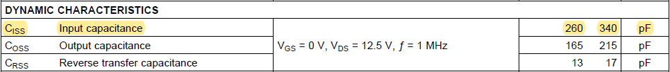
From the datasheet of the Diodes BSS138:

This seems to fit.

The design guide TIDUED0 of the reference design TIDA-010009 states:

2.3.2.6 Selecting Q1, Q2 and TVS Clamp for Surge Protection
The TPS26630 device supports the reverse input polarity protection feature. Connecting an N-channel
power FET (Q1) with the source to IN_SYS, drain to IN and GATE to B-GATE forms a back to back FET
topology in power path that is required to protect the load from input reverse polarity faults. Connecting an
external signal FET (Q2) across BGATE, DRV and IN_SYS creates a pulldown gate switch for Q1 during
reverse current and reverse polarity fault events.
In case of a negative surge strike, the input voltage will be clamped to –58.1 V by D1 resulting in a voltage
stress of –(58.1 V + 24 V) = 82.1 V, across the external blocking FET Q1. In this design a 100-V rated Nchannel
FET is chosen.
The B_GATE drive is in the range of 10 V – 14 V thus a suitable FET with the target RDS(on) specified at
this gate drive voltage is selected. Q2 should be at least 15 V VDS rated FET with a maximum VGS rating
of 20 V, Ciss ≤ 50 pF and VGTH(min) ≤ 3V. The CSD19533Q5A and CSD16301Q2 are selected for Q1
and Q2, respectively.

The datasheet of the MOSFET CSD16301Q2 nonetheless specifies:

The BSS138 is usually not specified for 3V logic level, but the CSD16301Q2 is.

Now I do want to know more about the DRV pins characteristic, what is its driving characterstics?

Can it drive the CSD16301Q2, but what are the pros and cons, when using this MOSFET?

Is it slower in shutting down the main reverse polarity MOSFET because of the much higher input capacitance?

Or will it nonetheless discharge the gate of the other MOSFET in less time because of its much lower and specified RDS(on) for 3V logic-level driving?

Looking forward to answers from the TI gurus.

  • Hi Friedl,

    Thanks for reaching out!

    TPS2663 can drive CSD16301Q2 FET but there would be slightly higher turn-on delay with CSD16301Q2 over BSS138 due to higher Ciss capacitance however the low Ron of CSD16301Q2 greatly reduces the t(Driver) time to discharge the VBGATE.

    I don't see a major concern or improvement with CSD16301Q2  as t(Driver) is generally 10% to 20% of tRCB(fast_dly) of 120 nsec (typical). Please proceed with BSS138 or CSD16301Q2 of your choice as per cost & size requirements.

    Best Regards, Rakesh

  • Dear Rakesh!

    That is all well and good, but does not really tell me more about the DRV pins characteristic.

    Can you give more details about the DRV pin, e.g. is it a current source, a MOSFET with RDS(ON)=x, max. drive Voltage y, .....and so on?

  • Hi Friedl,

    DRV pin is logic output pin with voltage high equal to 4.25 V (typ). Let me know if this answers your question.

    Best Regards, Rakesh

  • Dear Rakesh!

    What about its driving characteristic? Output resistance, min. max. voltage level of its supply voltage, ...

    Whatever is necessary to estimate the differences between different Mosfets driven by that pin.

  • Hi Friedl,

    3V (min), 4.25 V (typ) and 5.2V (max). I will check on the output resistance and update you.

    Best Regards, Rakesh

  • Hi Friedl,

    The output resistance is 133K 

    Best Regards, Rakesh