This thread has been locked.

If you have a related question, please click the "Ask a related question" button in the top right corner. The newly created question will be automatically linked to this question.

TPS61178: Operation of base part versus -1 part with min pulse width violation; with/without clock synch

Part Number: TPS61178
Other Parts Discussed in Thread: LM5155

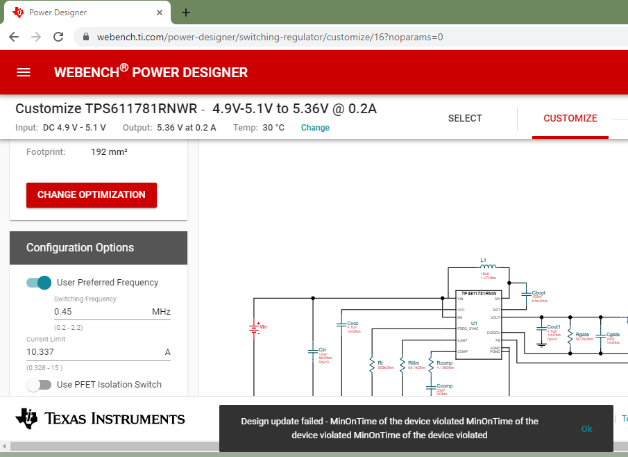
I saw a related question regarding Vout close to Vin.  In my situation I have Vin = (4.9 to 5.1), Vout = 5.36 @ 200 mA.  Will TPS61178 versus TPS611781 cause different results in Vout?

We originally wanted TPS61178 but this was out of stock so ordered the TPS611781.  A colleague reports abnormally high Vout  (about 5.9) and the FB pin is at 1.32V on one board.....not debugged yet.  Normally if violating minimum on time (with many boost ICs) I would expect pulse skipping but perhaps this device cannot do that (??)

Similarly; should I expect any impact in Vout (with minimum pulse width violation) if the TPS61178 or TPS611781 is synchronized to an external clock?

  • Hi Robert:

    The TPS611781 has the fixed switching frequency and no PFM. 

    But actually, both TPS61178 or TPS611781 can supply 5.36/2A with Vin from 4.9-5.1: 

    1. For tps61178, it has the PFM, so it will skips some pulses when Vin is too close to Vout to regulate the Vout to the target. 

    2, For TPS611781, the min Toff may cause the Vout higher than the target when Vin is too close the Vout. But you can set the switching frequency much lower to avoid such condition. 

  • Thank you, Minqiu

    I understand that lower frequency would avoid this issue, but I want to explore other options first.

    If TPS61178 is synchronized to 450 KHz will it PFM to regulate the voltage, or is it likely to produce overvoltage as with the TPS611781?

  • Hi Robert:

    I got your point. Please let me check in my lab. 

  • Thank you, Minqiu.  FYI we are working to product-ize a TI reference design so this has a lot of TI content.  The TPS61178 is one of many converters which we copied from the reference design but which I have tweaked.  One converter which I completely redesigned uses an LM5155.  There was some particular risk there as I have a new topology using a chip that I have never used.  We just applied power in the last week and it is going pretty well.  :-)

  • Hi Robert:

    Thanks for choosing TI. If there is any question during the evaluate, feel free to contact us.(But maybe support by different team.)

    For the TPS61178, I have checked in my lab, the Vout can regulate to the target well when Vin is close to Vout. With or without external clock. The converter mainly operate in the PFM mode with light load. 

    Would you share the waveform in your side? When you find Vout=5.9V not the 5.1V. Including the Vin, Vout, SW, and Vfb.

  • Thank you very much, Minqiu  Your response has been exemplary.

    This issue with the TPS611781 (versus TPS61178) has been observed by a colleague who is not a power supply engineer.  We are at different sites and are maintaining distance due to COVID and the fact that I am 68.  I do have one board on which I have been working with the LM5155-based converter.   Information from him yesterday suggests that the TPS611781 may have been synchronizing to a 1 MHz clock.  If that was happening, I guess that this higher frequency would have exacerbated the minimum duty cycle limitations based upon minimum pulse width.

    I hope that I can finish with this portion in a few days and then provide oscilloscope photos with the TPS611781.  However the clock signal is not something which I can work with (other than maybe to disconnect or disable it) as FPGA programming to change the clock frequency is not in my capability.  Anyway I will try to provide what I can.

    Thank you again.

  •  

     FP Bridge LV Conv test data P2 December 10 2020c.pdf

    I am attempting to attach test data including oscilloscope photos but this website is not cooperating.  In my lab I paste the oscilloscope photos into a Word document.  The Word document includes explanation and test conditions, etc.  Today now  I first tried to copy paste a section of my Word document including my scope photos.  That did not work.  Then I converted that page to .pdf and attempted to attach it above.  Based upon what I see here I am unsure whether this worked.  If this does not work, please send me your e-mail address to bobz@bioprober.com

    This is complicated as my colleague and I are working at different sites and with different skill sets.  But qualitatively we still have the same issues. I think we have decided to reduce frequency to 250 KHz to avoid minimum duty cycle issues.

    I would like to know:

    Can TPS61178 synchronize to an external clock input when the output is loaded for PWM operation?

    Also:  What does pin 1 impedance look like when driven by a 250 KHz clock?  I am experienced with many years of circuit design.  The TI reference design from which we started coupled the synch clock through a 220 nF capacitor as shown below.  I have removed this capacitor because it has proven to be a big source of our trouble.  But I want to replace it in such a way that the chip will synchronize to a clock when that is available, or free run when the clock is not available.  When pin 1 is driven by a clock input, what does the loading look like?  See below.  I found that simply driving a 250 KHz clock through C243 (reduced to 470 pF) does not work.  If pin 1 looked like a CMOS input (for example) then this method would probably work OK.  I  think I want to design something completely different but we are constrained by space.

    Thanks,

    Bob Zwicker

  • In my previous post when I was writing it appeared that the .pdf would not attach properly but the screen shot bmp worked OK.  Now after hitting the reply button it looks like the pdf is nicely attached but I doubt about the bmp screen shot.  Kindly confirm that you can view both images.

  • Hi Robert:

    Sorry, that too busy these days. Please allow me reply tomorrow. 

    I can see the pdf, but the image is missing. 

  • Thank you, Minqiu

    It was somewhat frustrating to post on this forum because as I wrote it seemed that neither method was working as expected.

    The images visible in the .pdf are the same as the images I tried to post as (I think it was a .bmp format screen shot.)  If you can view the two oscilloscope images in the .pdf, that is adequate.

  • Hi Robert:

    Firstly, please let me confirm that TPS611781 is the forced PWM device, while TPS61178 is auto PFM device.

    Then, TPS61178 can regulate the Vout even Vin is close to it, but the ripple will be larger than typical cases. 

    It can trigger the min Toff, and then the Vout will larger than target. But once the converter detect the Vout higher than target, it will skip some pulse to wait Vout drops to normal. Both internal clock or external clock.

  • For the pin1, the internal circuit is complexed and confidential. General, you can think there is a weak current source charge the RC circuit. When the voltage of the RC higher than reference, the output of the compactor will send out a pulse. 

    If there is an external clock, the output of the compactor is determined by the external signal.  

  • Thank you, Minqiu

    The one remaining question is this:  We would ideally like to have clock synch under heavy load but PFM under light load.  So:

    Can TPS61178 synchronize to an external clock input when the output is loaded sufficiently for PWM operation?

  • Hi Robert:

    Sorry for late reply. 

    For the TPS61178, I think it can regulate the Vout once Vin<Vout and the load is not too heavy. (All values should be within the recommend value in datasheet.)