This thread has been locked.

If you have a related question, please click the "Ask a related question" button in the top right corner. The newly created question will be automatically linked to this question.

LMG5200EVM-02: low efficiency at low Iout and current pulses even without input signal

Genius 12725 points
Part Number: LMG5200EVM-02

Hello Team,

I have 2 questions:

1) Can the efficiency be at 45% for these conditions:
Vin = 48V; Vout = 5V; Iout = 0.5A; Fsw = 2.5MHz ?

Measured input power 5.5W
output power: 0.5A x 5V = 2.5W

So power losses of 3W are bigger than output power...

See efficiency plot below measured on LMG5200EVM-02:

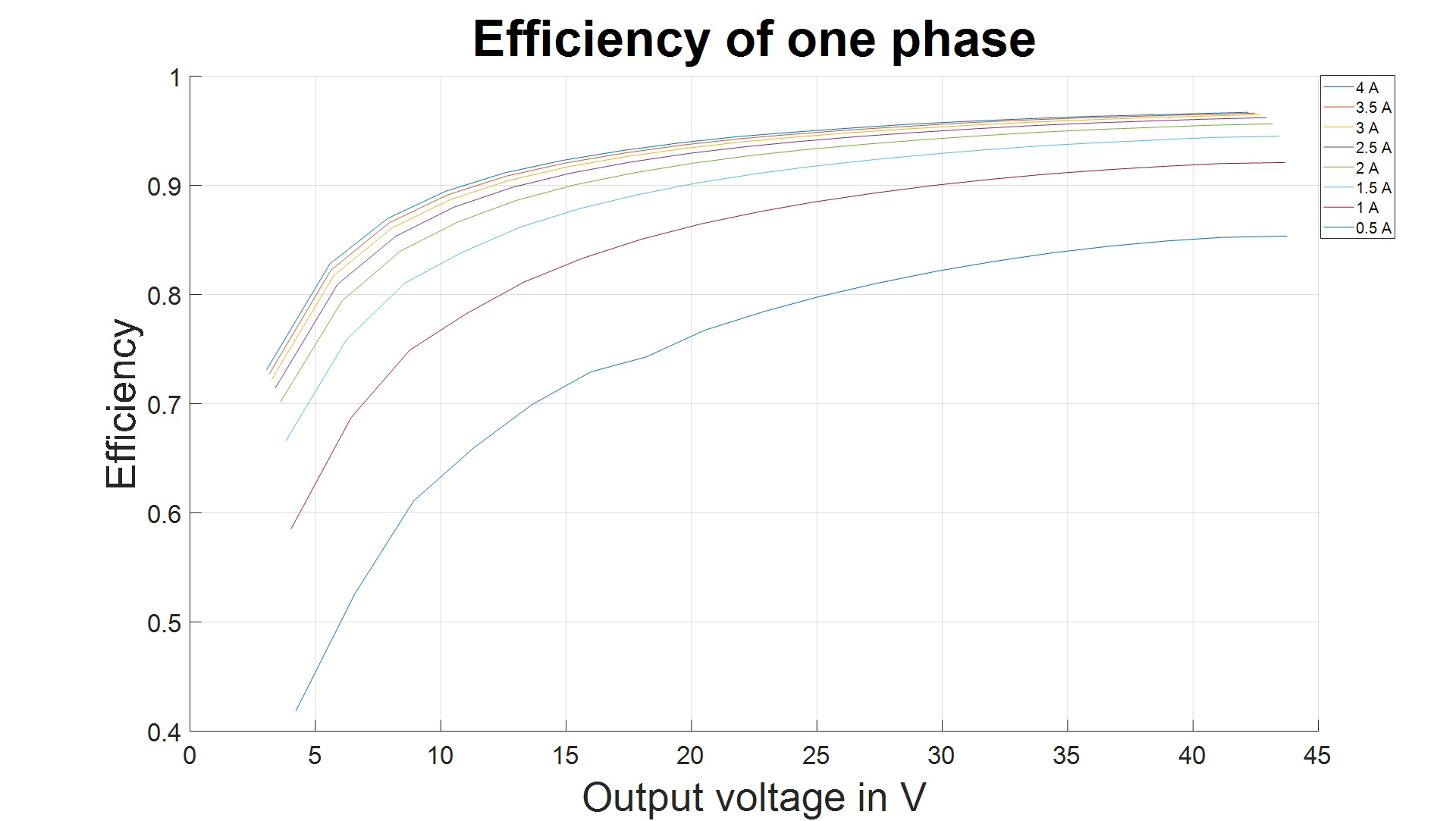
Is this poor efficiency at low output current expected? Can you explain why, please?

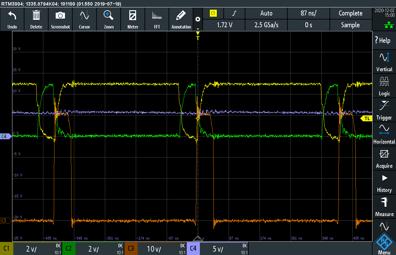
Also the control signals taken at TP9 and TP1 and switching node

2) Input current peaks up to 5A without any control signal at HI and LI:

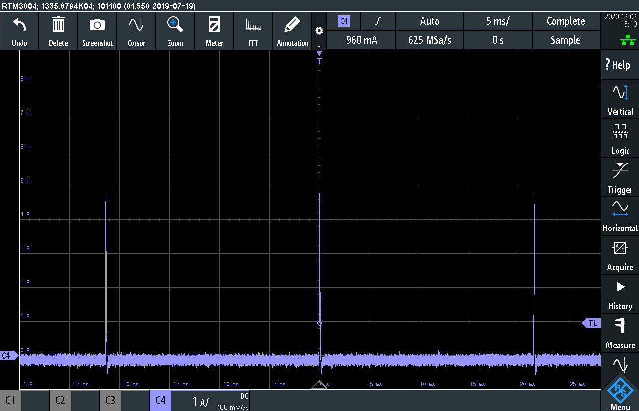
Can you explain where these peaks are coming from, please?

Any chance to remove them?

Thanks and Best Regards,

Hans

  • Hi Hans,

    Thanks for contacting us. At low current and low power operating condition, the switching loss and Coss loss will be dominating, especially at high switching frequency at 2.5MHz. We do expect the efficiency to be lower in such condition.

    From the first waveform we can see the low side is hard switched due to the low load current. One thing to try is to increase the value of R14 with low load current to increase the dead time for the low side signal. That way the switch node voltage can be discharged by the load current, and the loss should be decreased.

    For the second waveform, was it in a situation where HI and LI signals are both low? Could customer capture the switch node voltage and inductor current as well?

    Regards,

  • Hi Yichi,

    regarding the second waveform: The current pulses are visible for following conditions:

    • 48 V + 5V off
    • 48 V + 5 V + both control inputs open
    • 48 V + 5 V + both control inputs low

    Switch node voltage and coil current are displayed in the picture below.

    Channel 3 is the switch node voltage, Channel 2 the coil current and Channel 4 the current of the 48 V supply.

    Regards,

    Julian

  • Hello Julian,

    I don't have a good answer at this moment. During all these three conditions the GaN FET should be off and there should be no current draw. Also from the switch node waveform it doesn't look like there are signs of the FET conducting. 

    Could you probe the VIN (TP1 and TP7) to see anything you can find?

    Regards,