This thread has been locked.

If you have a related question, please click the "Ask a related question" button in the top right corner. The newly created question will be automatically linked to this question.

UCC27211: When the input voltage changes , will be the Driver(UCC27211) affected?

Part Number: UCC27211
Other Parts Discussed in Thread: UCC27282

During the experiment, an abnormal waveform of the IC was found.

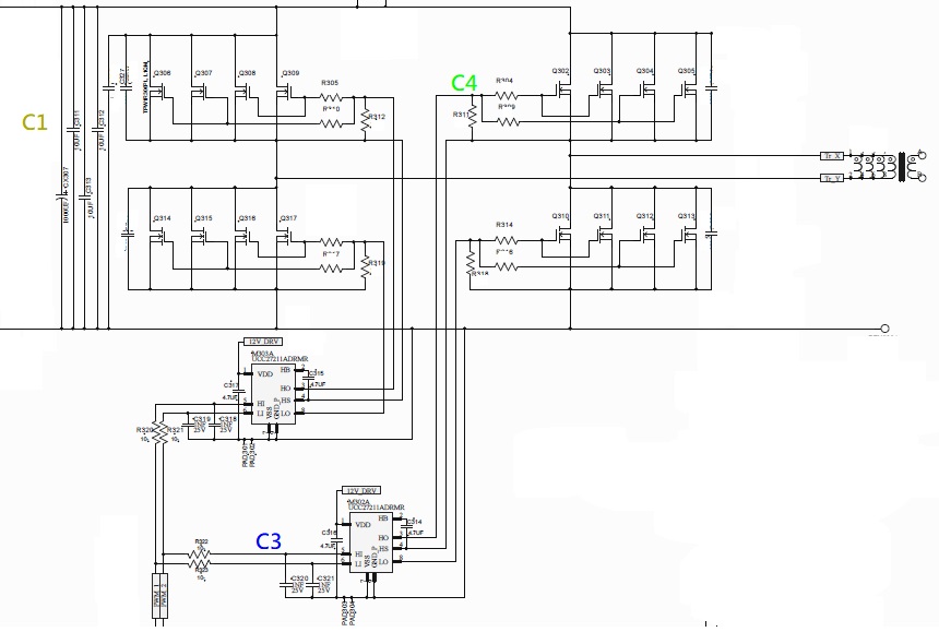
The test condition is input 11V to 14V, and the Vcc of the Driver IC is provided by the input.

Measure the waveform along the circuit, respectively measure C1: Input voltage, C2: DSP Output, C3: Isolated IC , C4: MOS Vgs (after Driver) 


The waveforms are as follows:

(C1:Vin, C2:DSP PWM, C3:Isolater IC to Diver, C4:Diver to MOS )

The result is as follows:

1. When Vgs is abnormally high, the DSP PWM is almost 0V, and the signal passing Isolated IC is slightly upward, so it should not be a problem with the DSP program.

2. From the previous cycle of PWM, it can be seen that the timing is DSP to Isolated IC to Vgs. It is reasonable to have a little delay time through an IC.

3. However, the Vgs of the abnormal waveform occurred slightly earlier than the Isolated IC signal, so it is judged that the problem may be caused by the abnormality of Driver IC.

Questions:

1.When the input voltage changes (11V to 14V), will be the Driver(UCC27211) affected? or other possible causes of abnormal waveform.

  • Hello Jim,

    Thanks for reaching out.

    So long as the driver's pins are within the recommended operating conditions, the driver may not misbehave and/or be affected by change on the VDD (11 to 14V). Can you confirm that C1 is measurement directly on the driver's VDD pin? If so, you may need to stabilize the supply with adequate capacitance values: 2 parallel capacitances (=0.1uF and >=1uF).

    I presume the issue is related to the high-side channel alone and not the low-side, please confirm?

    I have reviewed the schematic, can you please confirm your boot cap values to ensure that they're appropriately sized to drive 4 parallel FETs. When driving parallel FETs, we typically recommend allocating a resistor to each gate to dampen potential ringing at the gate due to asymmetric/uneven PCB traces.

    As for the waveform, your C1 signal appears to trigger the ringing on the VDD supply. If the issue is related to the high-side channel, the HB-HS will also be impacted in addition to VDD supply. Can you confirm the signals on HB-HS, on the same plot as HO-HS, HI and VDD?

    Regards,

    -Mamadou 

  • Thanks for your reply.

    1. Yes, VDD is on the same circuit loop. The capacitor used by VDD is 4.7UF.

    2. We measured abnormal waveforms, the high-side channel and the low-side have this problem.

    3. We use boot cap with a value of 4.7UF.  We have tested assigning a resistor to each gate, and this situation will happen again.

    4. Originally, the driver IC VDD and the input circuit had the same loop. We disconnected VDD from the input and provided an additional 12V power supply to get the following waveform:

    (C1:Vin, C2:Isolater IC to Diver, C3:LO-GND, C4:HO-HS )

    a. There will still be the problem of two overlapping signals, but significantly reduce the occurrence of cycle.

    b. In addition, we found that when the driver IC provides additional voltage(12V), HO-HS will increase the voltage along with abnormal conditions.

  • Hello You,

    Thank you for the additional information, and experiment. I see in your response that the VDD capacitor is 4.7uF and you mention the boot capacitor is 4.7uF. Can you confirm these are the values for VDD and boot capacitance?

    The boot capacitance value is very large which is a concern. I see the waveforms in one of the scope plots shows a switching frequency of ~83kHz, can you confirm if this is correct. I would recommend reviewing the boot cap value with the design guidance in the UCC27282 datasheet section 8.2. The MOSFET Qg, VDD and switching frequency determine the required boot cap value. This datasheet gives detail guidance on selecting component values. the datasheet link can be found below.

    https://www.ti.com/lit/ds/symlink/ucc27282.pdf?ts=1607525622618&ref_url=https%253A%252F%252Fwww.ti.com%252Fproduct%252FUCC27282

    Also the VDD capacitor is recommended to be 10x larger than the boot capacitor to minimized the VDD voltage drop from charging the boot capacitor.

    So I recommend confirming/resizing the boot capacitor and VDD capacitor to make sure the boot cap is not excessively large and VDD cap is 10x the value.

    The latest waveform behavior is usually cause by one of two reasons.

    1) there may be voltage disturbance on the gate driver inputs that can cause false triggering of the output. I would recommend trying a small R/C filter on the driver input pins, with the capacitor placed very close to the driver IC pins. Try an initial value of 33 ohms and 100pF which will not impact the delays very much. You can try increasing the values to see if this helps resolve the issue.

    2) there may be a Vgs perturbation from the MOSFET miller charge during the Vds rising edge that is high enough to momentarily false turn on the FET. One way to confirm, and resolve this is to slow down the switching dV/dt by increasing the turn on gate resistance to the MOSFETs. The lower dV/dt on the Vds will reduce the voltage disturbance on the FET Vgs from the miller charge.

    Confirm if this addresses your questions, or you can post additional questions on this thread.

    Regards,

  • Thanks for your reply.

    Yes, the boot cap we use is 4.7uF, and the switching frequency of the switch is 80k Hz, and we tried to increase the turn on gate resistance, with the same result.

    After your suggestions, we made the following adjustments. Change the boot cap to 0.47uF, and use the value of 33 ohms and 1nF R/C filter on the driver input pins, there will still be the same situation, as the following waveform:

    C1:Vin, C2:LO-GND, C3:HS-HO, C4:HB-HS(boot cap) 

    According to the results of the waveform diagram, we found that the waveform on the boot cap will also be abnormal, but it looks like HS-HO sends a turn on signal first, so that the voltage on the boot cap drops, then VDD charges the boot cap and its voltage rises.

    When there is ringing at the input, will the driver IC be abnormal? But we have disconnected the VDD of the Driver IC from the input, it will be affected only when the boot cap is discharged.

  • Hello You,

    Thank you for the additional information on the results with some changes. I want to clarify one signal, Vin, is this the VDD input to the driver?

    If so there does appear to be very high p-p noise especially in the area that you zoom the plots. You mention that you have disconnected VDD of the driver IC from the input. Does this mean that you disconnected from the bias supply on the board and are using an external bias voltage for the driver VDD? This part is not clear.

    If there is excessive noise on the driver VDD, there is risk of false tripping the driver UVLO which would result in unexpected behavior, this condition should be avoided.

    It looks like there could be noticeable noise injected into the driver VDD (if this is the Vin signal) or ground bounce, which is a concern for p-p noise on the driver bias, but also an indication that there could be ground noise at the driver IC pin affecting the driver pin signals, especially the driver inputs.

    Try, confirm some things to clean up the driver VDD noise. Try adding some resistance from the bias source to the driver VDD capacitor, this will act as a filter for VDD at the driver, try adding 5 to 10 Ohms in series with the driver VDD cap to the bias. Also try adding a high frequency capacitor in parallel with the VDD capacitor, 100nF if a good value for additional high frequency bypass. 

    I see that the boot cap was reduced significantly, but still confirm if the boot cap needs to be 0.47uF or can a lower value be adequate to drive the MOSFET Qg. A lower value boot capacitance, will charge faster from the VDD capacitance and have less voltage perturbation on VDD.

    Confirm that the VDD and HB capacitors are located close to the driver IC pins, connected with short traces.

    IF you continue to have concerns, I would suggest providing the schematic and layout of the driver and MOSFET areas of the circuit so I can provide additional, more detailed advice.

    Regards,

  • Thank for your reply.

    Yes, I have disconnected VDD of the driver IC from the input, and it had using an external bias voltage for the driver VDD.

    (C1: Vin, C2: Driver VDD, C3: HO-GND, C4: LO-GND)

    According to the result of the waveform, the same situation will occur when VDD and Vin are disconnected, but the number of occurrences decreases.

    We found that when there is an abnormal waveform, that voltage provided by the external VDD will drop down. But this should not affect the IC triggering UVLO function(Driver VDD > 10V).

    In addition, the voltage of HO and LO will change with Vin. What is the reason? I have disconnected Vin with VDD, and the voltage of VDD is stable.

  • Hello You,

    Thank you for the status update.

    For the question on the voltage of HO and LO will change with VIN, and what is the reason? I am not sure what you mean by the voltage will change, but let me comment. With higher VDD there is more available drive current on the driver output since there is a higher voltage on the internal driver output devices during the HO and LO switching transistions. You will usually see faster dV/dt on the gate drive signals with higher VDD on the driver. Confirm if this is the voltage change you are referring.

    It would be good to understand the relationship of the power train switch node waveform, or driver HS pin to ground, with respect to the unexpected pulses on the LO and HO outputs. Can you capture waveforms to show the switch node (HS pin), HO-HS driver output and LO driver output. Capture on a time base to see if the switch node transitions are happening close to the unexpected pulses.

    Have you tried R/C filters on the driver input pins? To confirm that there may not be some driver input signal disturbance that maybe was not clear on the scope plots? Try 22 Ohms and 100pF as a starting value.

    I am wondering if there is a gate drive trace/layout concern that may result in voltage perturbations on the Mosfet Vgs. Trace parasitic inductance can result in larger Vgs voltage disturbance from the Mosfet miller charge during switching. As an experiment, adding capacitance directly on the MOSFET gate and source pins helps reduce this Vgs disturbance. Can you try adding capacitance directly on the MOSFET gate and source pins of a value equal to the MOSFET Ciss?

    We are close to winter holidays so I want to mention that there will not be as much coverage until the new year.

    Confirm if this addresses your questions, or you can post additional questions on this thread.

    Regards,