This thread has been locked.

If you have a related question, please click the "Ask a related question" button in the top right corner. The newly created question will be automatically linked to this question.

BQ24192: EMI Issue

Part Number: BQ24192
Other Parts Discussed in Thread: BQ25792

Hi TI Team,

We are using BQ24192 charger chip on our custom board.

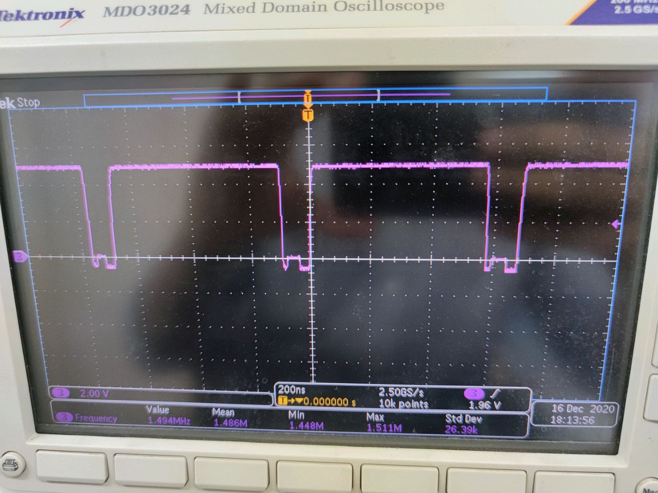
While doing inhouse EMI scan, we found that we are getting high radiation peaks on the charger chip switching frequency itself i.e. 1.5MHz. We are getting peaks at many harmonics of switching frequency.

In layout too, we have the smallest Switching loop.

Please help us on these.

  • HI Sahil,

    Attached is our layout and component recommendation for the BQ2419x family.  PMID bulk and decoupling capacitor is most important. Last resort, you can add a ferrite bead on the input or snubber on switch node.

    Regards,

    Jeff6012.bq2589xbq2419x_29xlayoutandEMIrecommendation.pdf

  • Hi Jeff,

    We have checked the recommended suggested by you.

    We are getting peaks at the fundamental frequency itself. Also, we don't have any ringing on the switching frequency, so I don't think Snubber circuit would be helpful in this case.

    Please see the attached waveform @ SW pin and picture of EMI scan.

  • Hi Sahil,

    Your oscope is 100MHz bandwidth so it is filtering out all frequencies above 100MHz, where the ringing would be.  You will need a higher frequency scope to see the ringing.

    Which EMI certification are you trying to meet?  The concern is usually at much higher frequencies than you are showing.

    Regards,

    Jeff

  • Hi Jeff,

    The frequency span was set to 30-100MHz, so we cannot observe peaks for greater than 100MHz. If we increase the frequency span, then we can see that too.

    We are trying to meet the FCC Part15B limits.

    I will share you the EMI waveform with increased frequency span soon.  Also, as per the SW pin waveform, there is no ringing. The waveform was captured with full load.

  • Hi Sahil,

    We will get back to you in the next business day.

    Thanks,

    Ning.

  • Hi Ning,

    Any update on this??

  • Hi Sahil,

    There will be significant noise at the charger's switching frequency of 1.5MHz and close harmonics.  There is no way to eliminate that.  The only way to prevent EMI at these lower frequencies may be a metal shield around the charger.  I assume you are using a shielded inductor?

    To protect against higher frequency EMI (>50 MHz), you can use ferrite bead on the input and/or decoupling capacitors at PMID pin and/or snubber on SW node.  

    Regards,

    Jeff

  • Hi Jeff,

    We are using shielded inductor.

    To dig in further, we captured the SW pin waveform using the high end oscilloscope and below is the waveform:

    Can you please help to get the expected waveforms? Seems to be Ground bouncing issue.

  • Hi Sahil,

    The waveform grounding is correct.  The SW node drops a diode drop below ground when the low side FET body diode is on, then the FET turns on, shorting the diode, and then the FET turns off and the diode is back on. 

    I am surprised that there is no ringing on the rising or falling edge. 

    Regards,

    Jeff

  • Hi Jeff,

    We don't have any ringing on rising or falling edge of SW pin waveform and we aren't having any EMI peaks due to that.

    We have EMI peaks on the fundamental frequency itself i.e. 1.5MHz. 

  • Hi Sahil,

    As I mentioned previously, all switching converters have EMI at their switching frequency. If your system can't handle that, you should change to a linear regulator based charger.  Or, if the EMI is frequency specific, then you might choose another charger than switching at a different frequency, like BQ25792 which has the choice of 1.5MHz or 750kHz.  The only other option is to place a metal shield around the IC and related components.

    Regards,

    Jeff